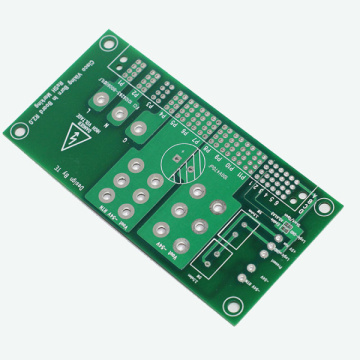
Double Sided PCB Tg150 High Frequency PCB
-
$1.02≥1 Piece/Pieces
- Min. Order:
- 1 Piece/Pieces
- Min. Order:
- 1 Piece/Pieces
Quantity:
Your message must be between 20 to 2000 characters
Contact NowBasic Info
Basic Info
Product Description
Product Description
Which surface treatment is best for PCB?
There are many types of circuit board surface treatments. PCB proofers should choose according to the performance and needs of the board. The following is a brief analysis of the shortcomings of various PCB surface treatments.

Tin spraying was a common treatment in the early days of PCBs. Now it is divided into lead spray tin and lead-free spray tin.
Advantages of tin spraying:
-->Longer storage time
-->After the PCB is completed, the copper surface is completely wetted (it is completely covered with tin before soldering)
-->Suitable for lead-free soldering
-->Mature technology
-->Low cost
-->Suitable for visual inspection and electrical measurement
Weaknesses of tin spraying:
-->Not suitable for wire binding; due to surface flatness, there are limitations on SMT; not suitable for contact switch design.
-->The copper will dissolve when spraying tin, and the board will withstand a high temperature.
-->Especially thick or thin boards have limitations in spraying tin, which makes the production and operation inconvenient.

Advantages of OSP:
-->The manufacturing process is simple and the surface is very flat, suitable for lead-free soldering and SMT.
-->Easy to rework, convenient production and operation, suitable for horizontal line operation.
-->The board is suitable for coexistence of multiple processing (for example: OSP+ENIG)
-->Low cost and environmentally friendly.
OSP weaknesses:
-->Limits on the number of reflow soldering (the film will be destroyed if the thickness of multiple soldering is thicker, basically there is no problem with the second time)
-->Not suitable for crimping technology, wire binding.
--> Visual inspection and electrical measurement are not convenient.
-->N2 gas protection is required for SMT.
-->SMT rework is not suitable.
-->High storage requirements.
3. Chemical silver
Chemical silver is a better surface treatment process.
Advantages of chemical silver:
-->Simple process, suitable for lead-free soldering, SMT.
-->The surface is very flat
-->Suitable for very fine lines.
-->Low cost.
Weaknesses of chemical silver:
-->High storage conditions, easy to contaminate.
-->Welding strength is prone to problems (microcavity problem).
-->Electromigration is prone to appear as well as Javanni bite corrosion on the copper under the solder mask.
-->Electrical measurement is also a problem
4. Chemical tin:
Chemical tin is the most copper-tin replacement reaction.
Advantages of chemical tin:
-->Suitable for horizontal production.
-->Suitable for fine line processing, suitable for lead-free soldering, especially suitable for crimping technology.
-->Very good flatness, suitable for SMT.
weakness:
-->Good storage conditions are required, preferably not more than 6 months, to control the growth of tin whiskers.
-->Not suitable for contact switch design
-->The production process has relatively high requirements for the solder mask process, otherwise it will cause the solder mask to fall off.
-->N2 gas protection is best when welding multiple times.
-->Electrical measurement is also a problem.
5. Chemical nickel gold (ENIG)
Nickel gold is a relatively large surface treatment process. Remember: the nickel layer is a nickel-phosphorus alloy layer. According to the phosphorus content, it is divided into high-phosphorus nickel and medium-phosphorus nickel. The application is different, so the difference is not introduced here.
Advantages of nickel gold:
-->Suitable for lead-free soldering.
-->The surface is very flat, suitable for SMT.
-->Through holes can also be coated with nickel and gold.
-->Long storage time, storage conditions are not harsh.
-->Suitable for electrical testing.
-->Suitable for switch contact design.
-->Suitable for aluminum wire binding, suitable for thick plates, strong resistance to environmental attacks.
6. Electroplated nickel gold
Electroplated nickel gold is divided into "hard gold" and "soft gold". Hard gold (such as gold-cobalt alloy) is commonly used on gold fingers (contact connection design), and soft gold is pure gold. Electroplating of nickel and gold is widely used on IC substrates (such as PBGA). It is mainly suitable for bonding gold and copper wires. However, the plating of the IC substrate is suitable. The bonded gold finger area needs to be electroplated with additional conductive wires.
Advantages of electroplating nickel gold:
-->Long storage time>12 months.
-->Suitable for contact switch design and gold wire binding.
-->Suitable for electrical testing
weakness:
-->The higher the cost, the thicker the gold.
-->Additional design lines are required for electroplating gold fingers to conduct electricity.
-->Because the thickness of gold is not constant, it may be too thick to cause embrittlement of the solder joints and affect the strength when used in welding.
-->The uniformity of the plating surface.
-->The electroplated nickel gold does not cover the edge of the wire.
-->Not suitable for aluminum wire binding.
7. Nickel Palladium (ENEPIG)
Nickel-palladium-gold is now gradually beginning to be applied in the PCB field, and it has been used more in semiconductors before. Suitable for bonding of gold and aluminum wires.
advantage:
-->Applied on the originality electronics IC carrier board, suitable for gold wire bonding and aluminum wire bonding. Suitable for lead-free soldering.
-->Compared with ENIG, there is no nickel corrosion (black plate) problem; the cost is cheaper than ENIG and electro-nickel gold.
-->Long storage time.
-->Suitable for a variety of surface treatment processes and stored on the board.
weakness:
-->The manufacturing process is complicated. Difficult to control.
-->The application history in the PCB field is short.

Printed boards have evolved from single-layer to double-sided, multi-layer and flexible, and still maintain their respective development trends. Due to the continuous development of high precision, high density and high reliability, continuous reduction of volume, cheap custom pcb fabrication, and improvement of performance, the printed board will still maintain a strong vitality in the future development of electronic equipment.
Summary of the domestic and foreign discussions on the future development trends of printed board manufacturing technology are basically the same, that is, to high density (HDI PCB), high precision (mulit-wiring printed board), fine aperture, fine wire, fine pitch, and high reliability. , Multi-layered, high-speed transmission, light weight, thinness direction development, in the production at the same time to improve productivity, low cost pcb manufacturing, reduce pollution, and adapt to the development of multi-variety, small-batch production. The technical development level of the printed circuit is generally represented by the line width, aperture, and thickness/aperture ratio of the printed board.


Related Keywords
Related Keywords
You May Also Like
You May Also Like