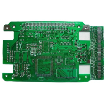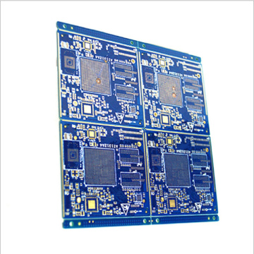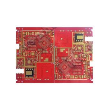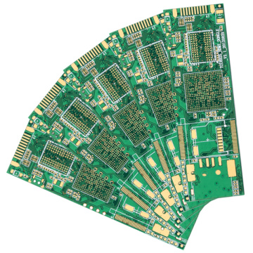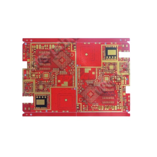


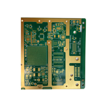
Multilayer PCB HDI Impedance Immersion Gold PCB&PCBA
-
$1.98≥1 Piece/Pieces
- Min. Order:
- 1 Piece/Pieces
- Min. Order:
- 1 Piece/Pieces
- Transportation:
- Ocean, Land, Air, Express
- Port:
- shenzhen
Your message must be between 20 to 2000 characters
Contact Now| Supply Ability: | 10000pcs/day |
|---|---|
| Payment Type: | T/T,Paypal |
| Incoterm: | FOB,EXW |
| Transportation: | Ocean,Land,Air,Express |
| Port: | shenzhen |
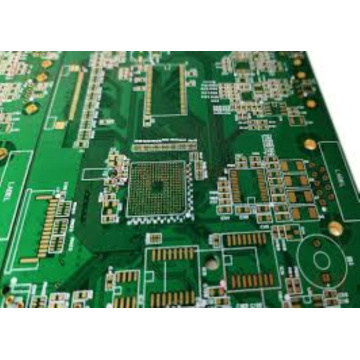
What is meant by characteristic impedance?
1. When the route is less than 25mm from the edge of the board, the characteristic impedance PCB is 1~4ohm smaller than the middle of the board, and when the route is more than 50mm from the edge of the board, the variation of the characteristic impedance value affected by the part is reduced, and the utilization rate of the board is considered. Under the prerequisite, it is proposed to choose the cutting specification first, considering the distance between the characteristic impedance line and the edge of the plate exceeding 25mm;
2. The most critical element that harms the uniformity of the characteristic impedance of the PCB circuit board is the uniformity of the thickness of the different parts, and the second is the uniformity of the graphic boundary;
3. The difference in the residual copper rate of different parts of the pcb circuit board will result in a characteristic impedance gap of 1~4ohm. When the pattern is spread and the uniformity is weak (the residual copper rate is very different), it is recommended that the characteristics of the electrical equipment are not harmed. Basically effectively pave the separation point of the blocking image and the electroplating process to reduce the difference in dielectric thickness and barrel thickness difference of different parts;
4. The lower the clamping force of the semi-dry solid sheet, the better the uniformity of the dielectric thickness after lamination. The flow of glue at the edge of the pcb circuit board will cause the dielectric thickness to be too small and the relative dielectric constant to be too large, which will lead to close The characteristic impedance value of the edge route of the board is lower than the middle area of the jigsaw;
5. For the inner route, the difference in the uniformity of the characteristic impedance PCB caused by the graphic boundary and copper thickness in the different parts of the board is small; for the surface route, the difference in copper thickness will harm the characteristic impedance within 2Ohm, but the difference in copper thickness The resulting difference in the boundary of the etching process pattern is very harmful to the uniformity of the characteristic impedance, and the uniformity function of the surface barrel plating needs to be improved.


Related Keywords