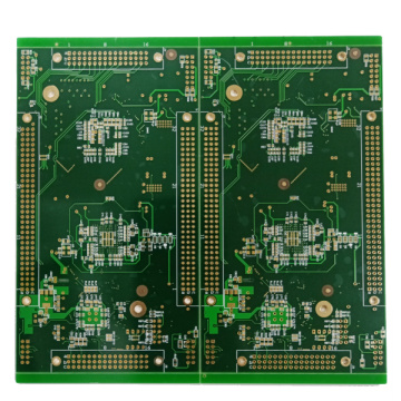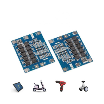


Customize Via in Pad PCB
-
$120.00≥1 Piece/Pieces
- Min. Order:
- 1 Piece/Pieces
- Min. Order:
- 1 Piece/Pieces
Your message must be between 20 to 2000 characters
Contact NowHow do I choose a PCB thickness?
Custom pcb fabrication might say that the standard PCB thickness is 1.57 mm, or about 0.062 inches. This is correct to a certain extent. Obviously, this is the size of the bakelite board manufactured in the early stage of PCB manufacturing, and the size has been fixed. Therefore, we can call it the historical standard PCB thickness. Today, PCB dimensions are larger or smaller than this standard, but this standard may still be the most common thickness in designs.
Nowadays, it is more accurate to say that there are a series of common or standard PCB thicknesses. These include 0.031 inches (0.78 mm), 0.062 inches (1.57 mm) and 0.093 inches (2.36 mm). Depending on your PCB manufacturing options and SMT&Through-Hole Assembly services, you may be able to manufacture circuit boards with other thicknesses. When determining PCB thickness, many of the following design and manufacturing factors need to be considered.


Related Keywords