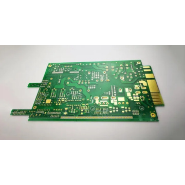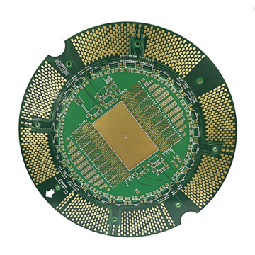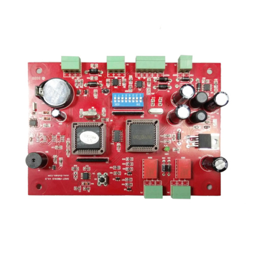
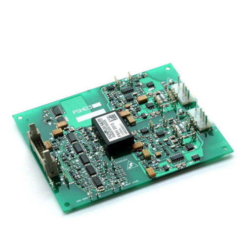

Double Layer Rigid UL ISO9001 Rigid PCB Board
-
$0.32≥1 Piece/Pieces
- Min. Order:
- 1 Piece/Pieces
- Min. Order:
- 1 Piece/Pieces
- Transportation:
- Ocean, Land, Air, Express
Your message must be between 20 to 2000 characters
Contact Now| Payment Type: | T/T,Paypal |
|---|---|
| Incoterm: | FOB,EXW |
| Transportation: | Ocean,Land,Air,Express |
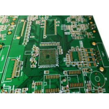
How to make a double-sided PCB?
The manufacturing process of double-sided pcb board
1. Preparation part: design the PCB, make the punching file, cut the PCB double-sided copper-clad board, then polish the double-sided copper-clad board for CNC drilling, and check whether there are defects after polishing and drying.
2. Making vias: This is the main link. Firstly, complete the hole. After the holes are organized and standardized, they are washed and dried through procedures such as washing and drying. After confirming that the holes are free of defects, black holes are carried out to prepare for the copper plating of the vias, then the through holes are carried out, and then the drying is carried out ( In order to fully blacken the air, water washing and drying must be performed twice). After completion, copper plating can be carried out. After copper plating, polishing is performed, and the holes are checked again for defects.
3. Line production process: applying photosensitive blue oil-drying ink-pasting the bottom, top line film, and positioning-proper exposure, development-washing, drying-checking whether there are defects in the line-tinning-washing-corrosion-fading Tin—on solder mask ink—dry ink—attach the film to the pad and set it in place—appropriate exposure—developing + check for defects—washing, drying—character ink, drying ink—sticking film, proper exposure—developing + inspection Defects-washing, drying-curing ink.
4. Mechanical forming treatment: cut off the excess parts to make a PCB board with Founder specifications, and then PCBA Manufacturing can solder Electronic Components to the PCB. After soldering the components, it can be energized for testing.

In the design of double-sided PCB boards, the layout of components and the wiring of circuit connections are the two key links. The layout is to put the circuit Electronic Components in the printed circuit board wiring area. Whether the layout is reasonable not only affects the subsequent wiring work, but also has an important impact on the performance of the entire circuit board. After ensuring the circuit functions and performance indicators, to meet the requirements of manufacturability, testing and maintenance, the components should be evenly, neatly and compactly placed on the PCB to minimize and shorten the leads and connections between the Electronic Components and Electronic connectors. , In order to get a uniform PCB assembly density.


Related Keywords