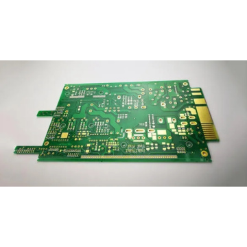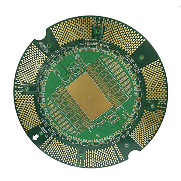

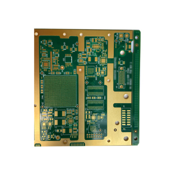
3 Oz Fr4 94V0 Copper Clad PCB Board
-
$0.32≥1 Piece/Pieces
- Min. Order:
- 1 Piece/Pieces
- Min. Order:
- 1 Piece/Pieces
Your message must be between 20 to 2000 characters
Contact NowHow to solder double-sided PCB?
In order to ensure reliable electrical conduction of the double-sided circuit board, the connection holes on the double-sided board (that is, the through-hole part of the metallization process) should be welded with wires or the like first, and the protruding part of the connecting wire tip should be cut to avoid stabs. Injury to the operator's hand, this is the preparation for the wiring of the board.

The selective soldering process includes: flux spraying, circuit board preheating, dip soldering and drag soldering. Flux coating process In selective soldering, the flux coating process plays an important role. When the soldering heating and soldering are finished, the flux should have sufficient activity to prevent the generation of bridges and prevent the circuit board from oxidizing. Flux spraying is carried by the X/Y manipulator to carry the circuit board through the flux nozzle, and the flux is sprayed onto the soldering position of the pcb circuit board.
Soldering circuit board skill 2:
The most important thing for microwave peak selective soldering after the reflow soldering process is the accurate spraying of the flux, and the micro-hole jet type will never contaminate the area outside the solder joints. The minimum flux point pattern diameter of micro-point spraying is greater than 2mm, so the position accuracy of the flux deposited on the circuit board by spraying is ±0.5mm to ensure that the flux is always covered on the welded part.
Circuit board soldering technique 3:
Wave Solder for PCBA can be compared with wave soldering to understand the process characteristics of selective soldering. The most obvious difference between the two is that the lower part of the circuit board is completely immersed in liquid solder in wave soldering, while in selective soldering, only Some specific areas are in contact with the solder wave. Since the circuit board itself is a poor heat transfer medium, it will not heat and melt the solder joints adjacent to the components and the circuit board area during soldering.


1. The electronic components that require shaping should be processed according to the requirements of the process drawing; that is, the shaping is first and then the plug-in.
2. After shaping, the model side of the diode should face up, and there should be no discrepancies in the length of the two pins.
3. When inserting devices with polarity requirements, pay attention to their polarity not to be reversed. Roll integrated block components, after inserting, no matter it is a vertical or horizontal device, there must be no obvious tilt.
4. The power of the soldering iron used for welding is between 25~40W. The temperature of the soldering iron tip should be controlled at about 242°C. If the temperature is too high, the tip is easy to "die", and the solder cannot be melted if the temperature is low. The soldering time should be controlled at 3 ~4 seconds.
5. During the formal welding, generally operate according to the welding principle of the device from short to high and from the inside out. The welding time should be mastered. If the time is too long, the device will be burnt, and the copper line on the copper clad board will also be burnt.
6. Because it is double-sided welding, a process frame or the like for placing the circuit board should also be made, so as not to squeeze the components underneath.
7. After the circuit board is soldered, a comprehensive check-in check should be carried out to check for missing insertion and soldering. After confirmation, trim the redundant device pins and the like on the circuit board, and then flow into the next process.
8. In the specific operation, the relevant process standards should be strictly followed to ensure the welding quality of the product.


Related Keywords