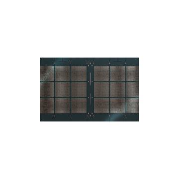


6 Layer laser Electronic PCB PCBA
-
$32.00≥1 Piece/Pieces
- Min. Order:
- 1 Piece/Pieces
- Min. Order:
- 1 Piece/Pieces
Your message must be between 20 to 2000 characters
Contact Now
What is the first step in PCB design?
1: Preliminary preparation for custom pcb fabrication
This includes preparing package libraries and schematics. Before proceeding with PCB design, we must first prepare the logic package of the schematic SCH and the package library of the PCB. The packaging library can be the library that comes with PADS, but it is generally difficult to find a suitable one. It is best to make your own packaging library based on the standard size information of the selected device. In principle, make the PCB package library first, and then make the SCH logic package. PCB packaging library requirements are high, which directly affects the installation of the board; SCH logic packaging requirements are relatively loose, as long as you pay attention to the definition of the pin attributes and the corresponding relationship with the PCB packaging.
2: PCB structure design
In this step, according to the determined circuit board size and various mechanical positioning, draw the PCB board surface in the PCB design environment, and place the required Electronic Components, Cable Connectors I/O Connectors, screw holes, assembly holes, etc. according to the positioning requirements . And fully consider and determine the wiring area and non-wiring area (such as how much area around the screw hole belongs to the non-wiring area).
3: Guide net table
It is recommended to import the board frame before the guide net table. Import DXF format frame or emn format frame
4: Rule setting
Reasonable rules can be set according to the specific PCB design. The rules we are talking about are PADS's constraint manager. Through the constraint manager, the line width and safety spacing are restricted at any link in the design process, where the constraint is not met. During subsequent DRC testing, it will be marked with DRC Markers.
The general rule setting is placed before the layout because sometimes some fanout work must be completed during the layout. Therefore, the rules must be set before the fanout. When the design project is large, the design can be completed more efficiently. Remarks: Setting rules is to complete the design better and faster, in other words for the convenience of the designer. The general settings are: 1. The default line width/line spacing of common signals. 2. Selection and setting of vias 3. Line width and color settings of important signals and power supplies. 4. Board layer settings.


Related Keywords