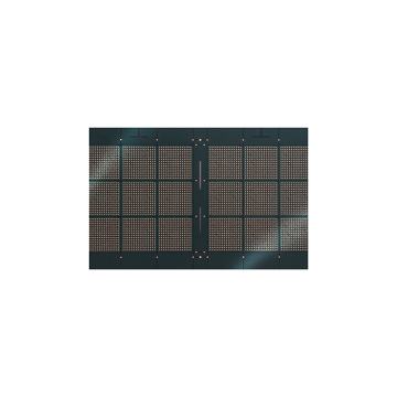


High Density print circuit board
-
$32.00≥1 Piece/Pieces
- Min. Order:
- 1 Piece/Pieces
- Min. Order:
- 1 Piece/Pieces
Your message must be between 20 to 2000 characters
Contact Now
What is HDI High Density Interconnect?
What is a high-density printed circuit board? It is the abbreviation of High Density Inverter, a BVH PCB with a relatively high line distribution density using micro-blind buried via technology.
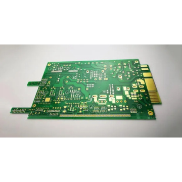
The printed circuit board is a structural element formed by insulating materials supplemented by conductor wiring. In PCBA Manufacturing, various Electronic Components will be installed on it. Therefore, PCB is a platform that provides the connection of Electronic Components, which is used to undertake the basis of connecting parts.
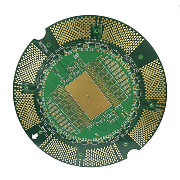
Under the pretext that electronic products tend to be multi-functional and complex, the contact distance of integrated circuit Electronic Components has been reduced, and the speed of signal transmission has been relatively increased. This is followed by an increase in the number of wiring and wiring between points. The length is locally shortened, which requires the application of high-density circuit configuration and micro-hole technology to achieve the goal. Wiring and jumper are basically difficult to achieve for single and double panels. Therefore, PCBs will become multilayered. Due to the continuous increase of signal lines, more power layers and grounding layers are necessary means for design. All these have made the Multilayer Printed Circuit Board (Multilayer Printed Circuit Board) more common.
For the electrical requirements of high-speed signals, the Characteristic impedance PCB must provide impedance control with alternating current characteristics, high-frequency transmission capabilities, and reduce unnecessary radiation (EMI). With the structure of Stripline and Microstrip, multi-layer design becomes a necessary design. In order to reduce the quality of signal transmission, insulating materials with low dielectric coefficient and low attenuation rate are used. In order to cope with the miniaturization and arraying of electronic components, the density of circuit boards is continuously increased to meet demand. The emergence of Surface-Mount (SMT) & BGA Assembly has promoted printed circuit boards to an unprecedented level of high density.
Therefore, most circuit board manufacturers call this type of product High frequency board or the full Chinese name "High Density Interconnection Technology". However, because of the smoothness of spoken language, some people directly call this type of product "high-density circuit board" or high frequency board.


Related Keywords