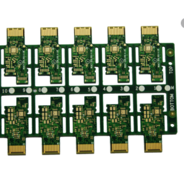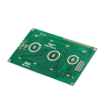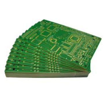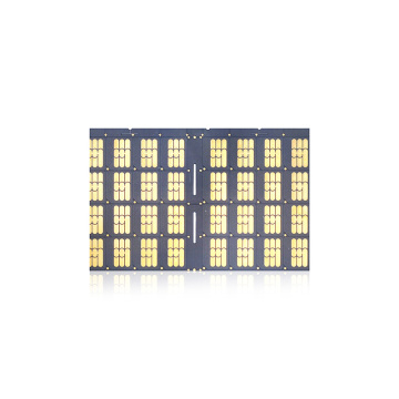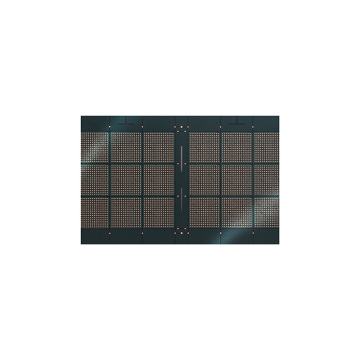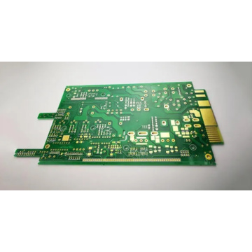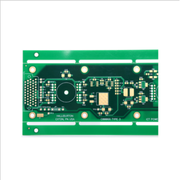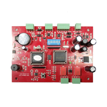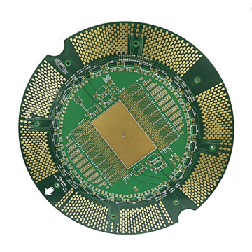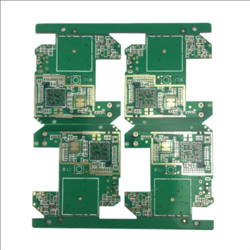
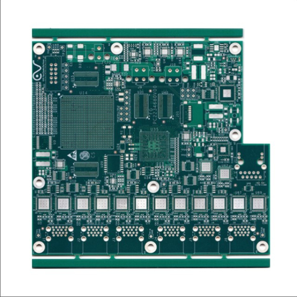
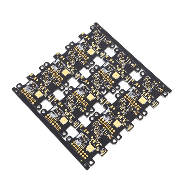
6 Layer Laser Circuits
-
$32.00≥1 Piece/Pieces
- Min. Order:
- 1 Piece/Pieces
- Min. Order:
- 1 Piece/Pieces
Your message must be between 20 to 2000 characters
Contact Now
Can you laser etch PCB?
In custom pcb fabrication, direct laser imaging simplifies the pcb manufacturing process by at least 60%, while traditional film image transfer requires more than a dozen steps. So what are the methods for direct laser imaging in the PCB manufacturing process? The LDI equipment equipped with High Quality Prototype PCB Fabrication all over the world belongs to the LDI of UV light, which can be divided into three types according to its process:
1) Direct laser imaging of photoresist. This type refers to the direct laser imaging of the in-process plate coated with a special photoresist. To complete the conductive pattern on the board is based on the following three steps:
The first step: Facilitate the LDI sensitization of the special photoresist directly on the plate by the laser. Laser sensitization is controlled by cad graphic data or graphic data stored in the computer for laser scanning, and the photosensitivity of professional photoresist is much stronger than that of traditional photoresist (about 10 times). Laser scanning can achieve high PCB graphics transfer productivity.
The second step: chemical development. The special photoresist still uses the traditional weak alkaline sodium carbonate solution for development.
The third step: chemical etching. Since the dedicated photoresist is acid resistant (or the acid resistance is stronger than the alkali resistance), it is necessary to use an acidic copper chloride etching solution for etching.
2) PCB production adopts electroless tinning laser direct imaging.
The laser direct imaging (LDI) of electroless tin plating on the board is also called laser direct engraving in some literature. This type refers to the use of chemical methods to plate a very thin anti-corrosion layer tin on the system board, and then use laser etching to remove the tin layer that does not need to be etched and protected, and the thickness of the lower part (3μm~5μm) of copper The foil is then chemically etched. Since the tin layer is 0.5μm~1.0μm thick), it is alkali and acid resistant.
3) Direct imaging with the laser on the copper-clad board. This type refers to the direct imaging of the laser only on the copper-clad board. He does not need to apply any anti-corrosion protection layer to the board, but directly uses laser etching to remove the unnecessary copper foil, but in order to damage the thickness of the medium, often leave a 3μm~5μm thick copper foil, and then perform strict The thickness of the copper foil left by the controlled rapid chemical etching. Therefore, the copper thickness of the copper conductor pattern on the board will be thinner. This specific problem is analyzed in detail.
In summary, we have learned about the type and method of laser direct imaging used in the PCB production process. The 6 Layer Laser Circuits process lies in excellence, continuous practice and optimization.

Related Keywords

