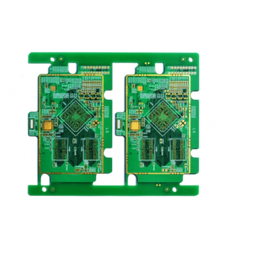


Roles of waste strip on PCB
-
$1.00≥1 Piece/Pieces
- Min. Order:
- 1 Piece/Pieces
- Min. Order:
- 1 Piece/Pieces
- Transportation:
- Ocean, Land, Air, Express, Others
- Port:
- shenzhen
Your message must be between 20 to 2000 characters
Contact Now| Payment Type: | T/T,Paypal |
|---|---|
| Incoterm: | FCA,EXW,FOB |
| Transportation: | Ocean,Land,Air,Express,Others |
| Port: | shenzhen |
Why PCB needs waste strip?
Although the waste strip is not the real element that constitutes a printed circuit board (PCB), it plays a very important role for a PCB assembled by surface mount technology (SMT). As the name suggests, the function of the waste strip is the same as the railway. A conveyor belt is used to transfer the PCB during the SMT assembly process for solder paste printing, pick and place, reflow/wave soldering and inspection. Unless the circuit board is accurately pasted to the conveyor belt through the process edge, the circuit board will never be transferred safely and effectively.
The main responsibility of the process side lies in its role as an "assisted" manufacturing, even if the manufacturability of the assembly is smoothly proceeded. This stems from the need for SMT placement machine rails to firmly fix the side of the circuit board and transfer it to the reflow oven. Therefore, if the design of the component is too close to the edge of the board, it may be "attacked" when picking, placing or soldering the component, resulting in errors or even failure. In addition to SMT assembly, this situation also applies to through-hole component assembly and wave soldering.
Why does PCB require the use of waste strip?
Although waste strip are of great significance to PCB assembly, not all PCBs must rely on it during assembly. After all, the production of waste strip leads to an increase in total cost. So, which type of PCB needs waste strip?
Generally speaking, two factors play a leading role in determining whether a waste strip is needed. Once any one of the conditions is met, the technical requirements must be carefully considered:
1. The distance between the component position and the edge of the circuit board. If the distance between the component and the edge of the circuit board is designed to be less than 3mm, the distance between the component and the edge of the PCB is so close that errors or malfunctions may occur. The waste strip is needed to expand the distance between the component location and the conveyor belt where the equipment is installed.
2. Reference mark. When there is no fiducial mark on the PCB, it is necessary to use the waste strip where the fiducial mark needs to be accurately implanted to ensure the correct coordinates so that the component position fully meets the requirements specified in the design document.
What should be considered on the waste strip?
1. The width of the waste strip. Generally speaking, according to specific assembly requirements and assembly equipment parameter requirements, the width of the waste strip is in the range of 1.5mm to 5mm. Therefore, it is very necessary to consult the contract assembler to ensure that your design is compatible with the corresponding assembly equipment.
2. The cost of the waste strip. With the manufacturing of waste strip, material consumption will definitely increase, so the total cost will also increase. How to balance PCB cost and manufacturability can be considered as the primary consideration for PCB design engineers and PCB manufacturers or assemblers. In order to minimize the cost, the usual method is to minimize the application of the waste strip by designing the best layout for the PCB panel, which can minimize the application of the waste strip. Reliable PCB manufacturers or assemblers have sufficient knowledge and experience to provide customers with ideal solutions based on quality and cost considerations.


Related Keywords