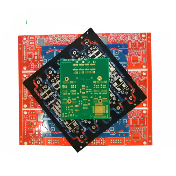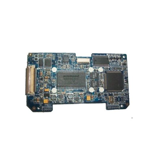
Impedance control and PCB design
-
$7.00≥2 Piece/Pieces
- Min. Order:
- 2 Piece/Pieces
- Min. Order:
- 2 Piece/Pieces
- Transportation:
- Ocean, Land, Air, Express, Others
- Port:
- Shenzhen
Your message must be between 20 to 2000 characters
Contact Now| Payment Type: | T/T,Paypal |
|---|---|
| Incoterm: | FOB,EXW,FCA |
| Transportation: | Ocean,Land,Air,Express,Others |
| Port: | Shenzhen |
What are the factors that affect PCB's impedance control?
Generally speaking, the factors that affect the characteristic impedance of the PCB: dielectric thickness H, copper thickness T, trace width W, trace spacing, dielectric constant Er of the material selected for the stack, and the thickness of the solder mask.
Generally speaking, the greater the dielectric thickness and line spacing, the greater the impedance value; the greater the dielectric constant, copper thickness, line width, and solder mask thickness, the smaller the impedance value.
The first one: the thickness of the medium. Increasing the thickness of the medium can increase the impedance, and reducing the thickness of the medium can reduce the impedance; different prepregs have different glue content and thickness. The thickness after pressing is related to the flatness of the press and the pressing procedure; for any kind of plate used, it is necessary to obtain the thickness of the medium layer that can be produced, which is conducive to the design and calculation, and the engineering design, pressing control, and incoming materials Tolerance is the key to media thickness control.
The second one: line width. Increasing the line width can reduce the impedance, and reducing the line width can increase the impedance. Line width control requires a tolerance of +/-10% in order to better meet the impedance control requirements. The gap of the signal line affects the entire test waveform, and its single point impedance is too high, making the entire waveform uneven, and the impedance line is not allowed to be compensated. The gap cannot exceed 10%. The line width is mainly controlled by etching control. In order to ensure the line width, according to the amount of etching side etching, light drawing error, and pattern transfer error, process compensation is performed on the engineering film to meet the line width requirements.
The third: copper thickness, reducing the line thickness can increase the impedance, and increasing the line thickness can reduce the impedance; the line thickness can be controlled by pattern plating or by choosing a base copper foil of corresponding thickness. The control of copper thickness is required to be uniform. The shunt block is added to the thin wire and isolated wire board to balance the current to prevent uneven copper thickness on the wire and affect the extremely uneven copper distribution on the cs and ss surfaces. The board should be crossed to achieve the goal of uniform copper thickness on both sides.
Fourth: the dielectric constant, increasing the dielectric constant can reduce the impedance, and reducing the dielectric constant can increase the impedance. The dielectric constant is mainly controlled by the material. Different boards have different dielectric constants, which are related to the resin materials used: FR4 boards have a dielectric constant of 3.9-4.5, which will decrease with the increase in frequency of use, and PTFE boards have a dielectric constant of 2.2- To obtain a high signal transmission between 3.9, a high impedance value is required, and thus a low dielectric constant is required.
Fifth: the thickness of the solder mask, printing on the solder mask will reduce the impedance of the outer layer. Under normal circumstances, one printing of the solder mask can reduce the single end by 2 ohms, and the differential can be reduced by 8 ohms, and the reduction of printing for two passes is twice that of one pass. When printing more than 3 times, the impedance value does not change.


Related Keywords

