

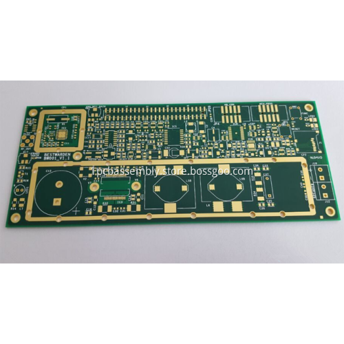

HDI PCB High Density Interconnect PCB Blind/Buried Vias
- Payment Type:
- T/T, Paypal, Money Gram, Western Union
- Incoterm:
- FOB, CFR, CIF
- Min. Order:
- 1 Piece/Pieces
- Min. Order:
- 1 Piece/Pieces
- Delivery Time:
- 5-30 Days
- Transportation:
- Ocean, Land, Air, DHL
- Port:
- Shenzhen, HongKong
Your message must be between 20 to 2000 characters
Contact Now| Place of Origin: | Shenzhen China |
|---|---|
| Productivity: | 500,000pcs per Month |
| Supply Ability: | 500,000pcs per Month |
| Payment Type: | T/T,Paypal,Money Gram,Western Union |
| Incoterm: | FOB,CFR,CIF |
| Certificate: | ISO9001, IATF16949, IPC-A-610F |
| HS Code: | 8517709000 |
| Transportation: | Ocean,Land,Air,DHL |
| Port: | Shenzhen,HongKong |
HDI PCB High Density Interconnect PCB Blind/Buried Vias
HDI PCB, it's High Density Interconnect PCB. It's the complicated multi-layer PCB with bury/blind vias which provided high density interconnect in PCB board. With the difficulty in bury/blind vias, it has different HDI Structure like 1+N+1, 2+N+2 and 3+N+3, etc. HDI, short for High Density Interconnection, is a type of printed circuit board technology starting to develop at the end of 20th century. For traditional PCB boards, mechanical drilling is utilized, with some disadvantages including high cost with aperture being 0.15mm and difficulty in improvement as a result of the influence of drilling tool. However, for HDI PCBs, laser drilling is utilized and as soon as it was introduced, it received massive popularity. HDI boards are also called laser boards whose aperture is ordinarily in the range of 3.0-6.0mil (0.076-0.152mm) and line width 3.0-4.0mil (0.076-0.10mm), which results in the fact that the pad size can be drastically decreased so that more layout can be arranged in each unit area. HDI technology adapts and pushes the development of PCB industry and now HDI circuit boards have been massively applied in all kinds of devices.
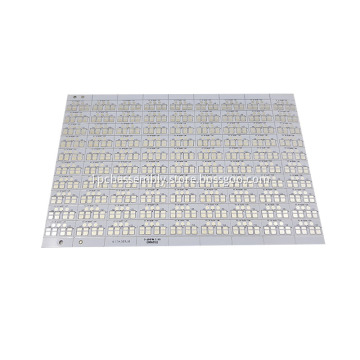
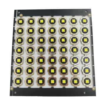
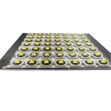
PCB Manufacture Show

PCB Assembly Show

Our Services:
1. PCB Design: One-stop EMS manufacturer, speciallized in designing wireless charging PCBA, bluetooth earphone & Voice box PCBA and other consumer electronics products.
2. PCB Manufacture: Standard FR4 1-36layer PCB, Flex PCB, Rigid-Flex PCB, HDI PCB, Rogers PCB, Metal Core PCB, etc.
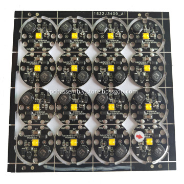
3. PCB Assembly: SMT and THT assembly, available for 01005, fine pitch and BGA assembly.
4. Components Sourcing: Available to source all components shown in BOM file (BOM Kitting), hard to find components and long lead time components, etc.
5. One-Stop Turnkey PCBA Manufacture: PCB design+PCB Manufacture+Components Sourcing+PCB Assembly+Electronic Assembly, or PCB Manufacture+Components sourcing+PCB Assembly, etc.
Technical Capabilities:
|
PCB Manufacture Capabilities |
|
|
Layers |
1-36 layers |
|
Material |
FR-4 (Standard FR4, Mid-Tg FR4, Hi-Tg FR4, Lead free assembly material) , Polymide, Metal Core, Rogers, etc. |
|
Board Thickness |
0.1mm-6.0mm (.016"-.126") |
|
Copper Thickness |
1/2oz-6oz(18um-210um) |
|
Board size |
600mm*1200mm |
|
Min Tracing/Spacing |
0.075mm/0.075mm (3mil/3mil) |
|
Min drilling Hole diameter |
0.15mm(6mil), 0.1mm(4mil)-laser drill |
|
Solder Mask |
LPI, different colors(Green, Green matt, Black, Black Matt, White, Red, Yellow, Blue) |
|
Silkscreen color |
White, Blue, Black, Red, Yellow |
|
Surface finish |
Lead free HASL, immersion gold, golden finger, immersion tin, immersion silver, OSP, Carbon oil, plated hard gold(up to 100u") |
|
Impedance tolerance |
+/-5%~+/-10% |
|
Chamfer of Gold Fingers |
20, 30, 45, 60 |
|
Test |
Flying probe or Testing fixture |
|
PCB Assembly Capabilities |
|
|
Quantity |
From prototype to big volume, no MOQ |
|
Assembly type |
SMT, THT or Hybrid |
|
Parts procurement |
Full turnkey (we provided all components) |
|
Partial turnkey ( Customer provide the main components and we provide the rest) |
|
|
Kitted (Customer provide all components) |
|
|
Component types |
SMT 01005, BGA 0.3mm pitch, QFP 0.3mm pitch, etc. |
|
Test |
Custom testing, ICT, FCT, AOI, Test jig |
Our Team and Office:

Our PCB Manufacture Factory:

Our PCB Assembly Factory:

FAQ:
Q: What files need for custom PCB manufacture?
A: Gerber or .pcb or .pcbdoc or .brd file is required.
Q: What files need for custom PCB assembly order?
A: Gerber and the BOM files are required, if you have pick&place file, send it to us as well.
Q: What is payment terms acceptable?
A: For new customer and the total amount within 10000usd, 100% payment in advance by PayPal or T/T or WU. For total amount beyond 10000usd, please contact us.
Q: What files need for PCB/PCBA clone services?
A: For PCB/PCBA clone service, send us the pictures for evaluate first, and we will need 1-2 samples of the PCB/PCBA board for copying.
Related Keywords


