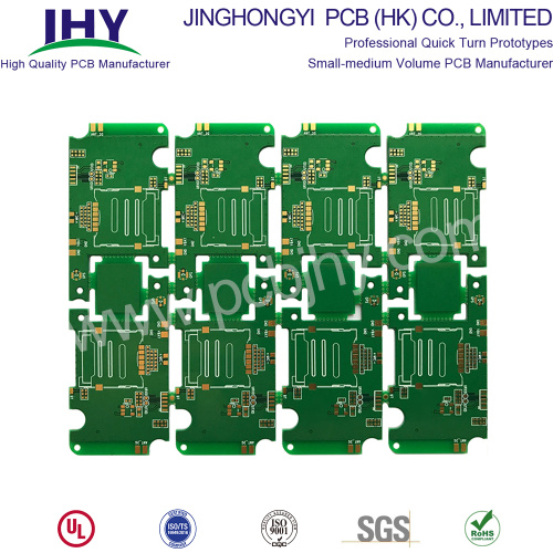

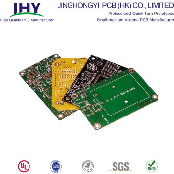
Rapid PCB prototyping services for 8 layer PCB
- Payment Type:
- L/C, T/T, D/P, Paypal, Money Gram, Western Union
- Incoterm:
- FOB, CFR, CIF, FCA, CPT
- Min. Order:
- 1 Piece/Pieces
- Min. Order:
- 1 Piece/Pieces
- Transportation:
- Ocean, Air
Your message must be between 20 to 2000 characters
Contact Now| Place of Origin: | China |
|---|---|
| Productivity: | 10000 |
| Payment Type: | L/C,T/T,D/P,Paypal,Money Gram,Western Union |
| Incoterm: | FOB,CFR,CIF,FCA,CPT |
| Certificate: | ISO9001 |
| Transportation: | Ocean,Air |
Rapid PCB prototyping services for 8 layer PCB with high quality and low cost.
PCB prototype manufacturing is the most economical solution to reduce the irreversible problems of products after formal batch production, resulting in incalculable economic losses.
Jinghongyi PCB can produce single-sided PCB, 2-layer PCB, 4-layer PCB, 6-layer PCB, 8-layer PCB, 10-layer PCB and even more layers of multi-layer PCB prototype and small and medium-sized mass production for customers.
Among them, the manufacturing of 8-layer circuit boards is more complex, difficult and relatively high cost. However, we generate a lot of 8-layer circuit boards. Therefore, your 8-layer circuit boards should be manufactured by reliable and experienced manufacturers like us. Moreover, there is no minimum quantity limit here. We can start with 1pcs. Most importantly, we offer higher quality products and more reasonable prices. There are few PCB manufacturers in the world who think about customers like us.
We support a 24-hour, 48-hour, 72-hour rush to solve your urgent needs.
Three common 8-layer PCB stacking modes
1. The first 8-layer PCB stacking mode
This is not a good stacking method because of the poor electromagnetic absorption capacity and power impedance. Its structure is as follows:
Layer 1: Signal 1, Component Surface and Microstrip Line Layer
Layer 2: Signal 2, Internal microstrip alignment layer, better alignment layer (X direction)
Layer 3: Ground
Layer 4: Signal 3, Strip line layers, better line layers (Y direction)
Layer 5: Signal 4. Strip line alignment layer
Layer 6: Power
Layer 7: Signal 5, Internal microstrip alignment layer
Layer 8: Signal 6, Microstrip alignment layer
2. Another 8-layer PCB stacking method
Due to the addition of reference layer and good EMI performance, the impedance of each signal layer can be well controlled. Its structure is as follows:
Layer 1: Signal 1, Component Surface, Microstrip Line Layer, Good Line Layer
Layer 2: Ground, Grounding Layer, Better Absorption Ability of Electromagnetic Wave
Layer 3: Signal 2, Strip line layers, good line layers
Layer 4: Power, The power supply layer and the underlying stratum constitute excellent electromagnetic absorption
Layer 5: Ground, Grounding Layer
Layer 6: Signal 3, Strip line layers, good line layers
Layer 7: Power, Grounding layer, with large power supply impedance
Layer 8: Signal 4, Microstrip alignment layer, good alignment layer
3. The third 8-layer PCB stacking method is also the best one we recommend.
The multi-layer grounding reference plane is adopted in this stacking mode, so it has very good magnetic absorption capacity. The structure is as follows:
Layer 1: Signal 1, Component Surface, Microstrip Line Layer, Good Line Layer
Layer 2: Ground, Grounding Layer, Better Absorption Ability of Electromagnetic Wave
Layer 3: Signal 2,Strip line layers, good line layers
Layer 4: Power, The power supply layer and the underlying stratum constitute excellent electromagnetic absorption
Layer 5: Ground, Grounding Layer
Layer 6: Signal 3, Strip line layers, good line layers
Layer 7: Ground, Grounding Layer, Better Absorption Ability of Electromagnetic Wave
Layer 8: Signal 4, Microstrip alignment layer, good alignment layer
Of course, for choosing how to use several layers of boards and how to stack them, many factors should be considered, such as the number of signal networks on the circuit board, the density of components, the density of PIN, the frequency of signals, the size of boards and so on. We should consider these factors comprehensively. The more the number of signal networks, the greater the density of components, the greater the PIN density, and the higher the frequency of signals, the design of multi-layer board should be adopted as far as possible. In order to get good EMI performance, it is best to ensure that each signal layer has its own reference layer.
Sometimes we will encounter a term: false 8-layer PCB, which is not really an 8-layer PCB, but a 6-layer PCB. In order to meet the impedance and thickness requirements of the circuit board, the 6-layer PCB uses three core boards, and the number of 8-layer PCB core boards is the same, so it is called false 8-layer PCB. In addition, fake 8-layer PCB will cost more than conventional 6-layer PCB, so we suggest either accepting fake 8-layer PCB or changing 6-layer PCB to 8-layer PCB.
If you want more information, these two pages may help you: 8 Layer PCB Stackup Guidelines, 8 layer PCB manufacturing
8 Layer PCB manufacture Price
For ordinary graphics cards and motherboards, the use of 4-layer PCB can basically meet the needs, and the cost of 6-layer PCB is about twice that of 4-layer PCB. 8-layer PCB is four times that of 4-layer PCB. Therefore, the general customers use 4-layer PCB.
However, it is undeniable that this is to some extent a cost-saving way, but at the expense of product stability.
Because if we use 6 or 8-layer PCB, we can have enough wiring space and more consideration of ground wire and power supply. So, we don't need to be too strict with the tightness of wiring. In this way, the line width and electromagnetic interference between wires will be fully considered. The stability of the board is obviously better than that of the 4-layer printed circuit board. Of course, this can not be generalized, because different wiring engineers have different levels and abilities.
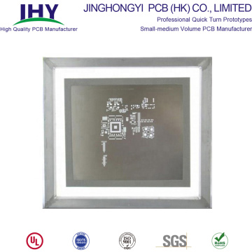
PCB prototype fabrication


Prototype PCB Manufacturing Capability
Learn more about JHY PCB by exploring the manufacturing capability of PCB Prototype below. We can do more than you can imagine.
|
Item |
Manufacturing Capability |
|
Number of Layers |
1 - 8layers |
|
Order Quantity |
5pcs - 100pcs |
|
Laminate |
FR-4 Standard |
|
Maximum PCB Size(Length x Width) |
600*1000mm |
|
Board Dimensions tolerance |
±0.1mm - ±0.3mm |
|
Board Thickness |
0.4mm - 4mm |
|
Board Thickness Tolerance |
±0.1mm - ±10% |
|
Copper Thickness |
1-6OZ |
|
Min Tracing/Spacing |
2mil/2mil |
|
Solder Mask Color |
Green, White, Blue, Black, Red, Yellow |
|
Silkscreen Color |
White, Black |
|
Surface Finish |
HASL, LF HASL, ENIG |
|
Test |
Flying probe, Testing Fixture |
Why choose us?
- Save money&time! Achieve peace of mind!
- A professional and trustworthy PCB prototype manufacturer.
- Fastest PCB Prototype.
- One stop solution for various PCB&SMT Stencil.
- Low cost for simple PCB.
- Affordable price for high-tech PCB.
- Minimum orders 1pcs.
- 24-hour online customer service.
- Professional PCB engineer for one-to-one service.
- Shipment on time.
- Guarantee good service and quality from PCB quotation to delivery.
Certification(UL:E466618, TS16949, ISO9001.RoHS)
 |
 |
 |
PCB Shipment
JHY PCB offers flexible shipping methods for our customers, you may choose from one of the methods below.

JHY PCB 's Packing Way
- Use one professional PCB vacuum bag, with desiccant inside. Vacuum compressed totally.
- Paste label and RoHs mark. Use second vacuum bag to protect boards again, vacuum compressed, make sure no exception.
- Microsection report and Tin testing board are put together with PCB in cartons.COC (Certificate of Conformity) will be sent to customer by email in PDF.
- Several layers of thick EPE(Expandable polyethylene) are filled fully in gaps between PCBs and cartons. The thickness of 1 layer EPE is 10mm.
- Neutral Packing is adopted if no special requirements. Strong and thick cartons(Thickness:10mm,7 layers). Different sizes of cartons are designed to meet the demand of different PCB size. All package are within weight limit of cartons. For mass production order, no exceed 21kg per carton normally.
- All cartons sealed with strong adhesive tape should be sealed twice so as to make them more durable.
- Solid PP/PET strapping is used outside of cartons.
- Shipping mark, fragile mark and postcode label are all pasted clearly.
Related Keywords
-

PCB Assembly SMT PCB Stencil PCB Stencil Maker

High Quality 24V LED PCB Circuit Board Assembly

Customized Single-sided 12V SMD LED PCB Circuit Board
Related ProductsProduct Categories-
PCB Prototype(97)
-
Quick Turn PCB(33)
-
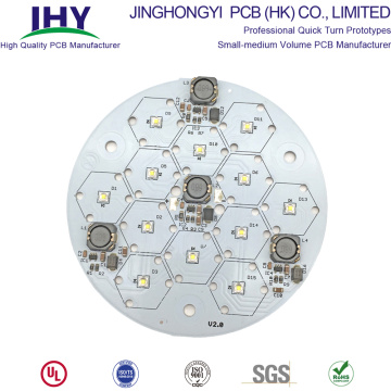
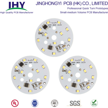
LED PCB(114)
-
Single Sided PCB(15)
-
Double Sided PCB(60)
-
Multilayer PCB(149)
-
Rigid PCB(22)
-
Flexible PCB(48)
-
Rigid Flex PCB(43)
-
Aluminum PCB(62)
-
Metal Core PCB(50)
-
Thick Copper PCB(106)
-
HDI PCB(61)
-
Impedance Control PCB(27)
-
BGA PCB(11)
-
High TG PCB(32)
-
Fr4 PCB(44)
-
Gold Fingers PCB(29)
-
PCB Application(5)
-
PCB Stencil(56)
-
PCB Assembly Service(67)
-
High Frequency PCB(47)