

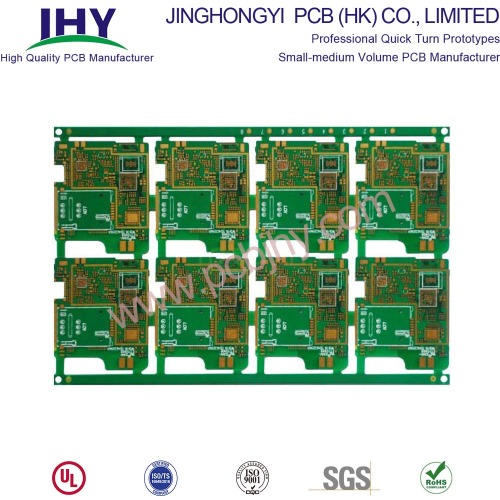
8 Layer 1+N+1 HDI PCB
- Payment Type:
- L/C, T/T, D/P, Paypal, Money Gram, Western Union
- Incoterm:
- FOB, CFR, CIF, EXW, FCA, CPT, CIP
- Min. Order:
- 1 Piece/Pieces
- Min. Order:
- 1 Piece/Pieces
- Transportation:
- Ocean, Air
Your message must be between 20 to 2000 characters
Contact Now| Place of Origin: | China |
|---|---|
| Productivity: | 10000 |
| Payment Type: | L/C,T/T,D/P,Paypal,Money Gram,Western Union |
| Incoterm: | FOB,CFR,CIF,EXW,FCA,CPT,CIP |
| Certificate: | ISO9001 |
| Transportation: | Ocean,Air |
Name: 8 Layer 1+N+1 HDI PCB Board
Material: FR-4
Layer: 8 Layer 1+N+ HDI
Color: Black, White
Finished Thickness: 0.8mm
Copper Thickness: inner: 1OZ, ourter: 0.5OZ
Surface Treatment: Immersion Gold+OSP
Min Trace / Space: 3mil/3mil
Min Hole: Mechanical hole 0.2mm, Laser hole 0.1mm
Application: Micro electronic products

The materials we use to produce HDI PCB include: FR4 standard, FR4 high performance, Halogen free FR4, Rogers
Surface finishes available OSP, ENIG, Immersion tin, Immersion silver, Electrolytic gold, Gold fingers.
Our advantage: Multilayer boards with a higher connection pad density than standard boards, with finer lines/spaces, smaller via holes and capture pads allowing microvias to only penetrate select layers and also be placed in surface pads.
For more information about the HDI PCB and the production capacity of our HDI circuit board, please download the PDF file provided by us.
High Density Interconnects (HDI) board are defined as a board (PCB) with a higher wiring density per unit area than conventional printed circuit boards (PCB).
HDI PCB Full Forms:
1+N+1, 2+N+2, 3+N+3, 4+N+4, Any Layer Interconnection
According to layer up different, currently DHI PCB board is divided into three basic types:
1+N+1, 2+N+2, Any Layer Interconnection

1) HDI PCB (1+N+1)
Features:
Suitable for BGA with lower I/O counts
Fine line, microvia and registration technologies capable of 0.4 mm ball pitch
Qualified material and surface treatment for Lead-free process
Excellent mounting stability and reliability
Copper filled via
Application: Cell phone, UMPC, MP3 Player, PMP, GPS, Memory Card
1+N+1 HDI PCB Structure:

2) HDI PCB (2+N+2)
Features:
Suitable for BGA with smaller ball pitch and higher I/O counts
Increase routing density in complicated design
Thin board capabilities
Lower Dk / Df material enables better signal transmission performance
Copper filled via
Application: Cell phone, PDA, UMPC, Portable game console, DSC, Camcorder
2+N+2-HDI-PCB-structure

3) ELIC (Every Layer Interconnection)
Features:
Every layer via structure maximizes design freedom
Copper filled via provides better reliability
Superior electrical characteristics
Cu bump and metal paste technologies for very thin board
Application: Cell phone, UMPC, MP3, PMP, GPS, Memory card.
Every Layer Interconnection Structure

The HDI circuit board has the following advantages:
- lower costs
- increase wiring density
- is conducive to the use of advanced packaging technology
- have better electrical performance and signal accuracy
- reliability is better
- can improve the thermal properties
- can improve radio frequency interference, electromagnetic wave interference, electrostatic discharge
- increase design efficiency
Related Keywords
-

Customized Single-sided 12V SMD LED PCB Circuit Board

HDI Fr4 Tg130 Tg150 Tg170 Tg180 Multilayer PCB

Shenzhen 10 Layer Gold Finger PCB Manufacturing
Related ProductsProduct Categories-
PCB Prototype(97)
-
Quick Turn PCB(33)
-
LED PCB(114)
-
Single Sided PCB(15)
-
Double Sided PCB(60)
-
Multilayer PCB(149)
-
Rigid PCB(22)
-
Flexible PCB(48)
-
Rigid Flex PCB(43)
-
Aluminum PCB(62)
-
Metal Core PCB(50)
-
Thick Copper PCB(106)
-
HDI PCB(61)
-
Impedance Control PCB(27)
-
BGA PCB(11)
-
High TG PCB(32)
-
Fr4 PCB(44)
-
Gold Fingers PCB(29)
-
PCB Application(5)
-
PCB Stencil(56)
-
PCB Assembly Service(67)
-
High Frequency PCB(47)


