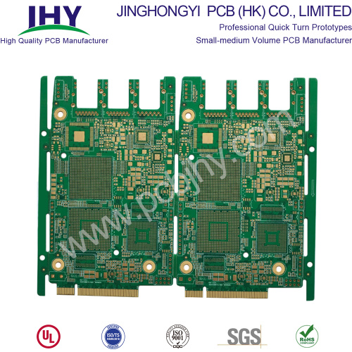
HDI Technology PCB Prototype
- Payment Type:
- L/C, T/T, D/P, Paypal, Money Gram, Western Union
- Incoterm:
- FOB, CFR, CIF, EXW, FCA, CPT, CIP
- Min. Order:
- 1 Piece/Pieces
- Min. Order:
- 1 Piece/Pieces
- Transportation:
- Ocean, Air
Your message must be between 20 to 2000 characters
Contact Now| Place of Origin: | China |
|---|---|
| Productivity: | 10000 |
| Payment Type: | L/C,T/T,D/P,Paypal,Money Gram,Western Union |
| Incoterm: | FOB,CFR,CIF,EXW,FCA,CPT,CIP |
| Certificate: | ISO9001 |
| Transportation: | Ocean,Air |
HDI Technology PCB Prototype
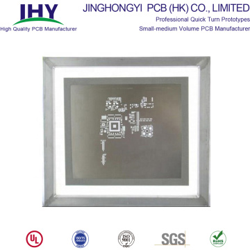
HDI PCB (High Density Interconnector PCB), HDI Technology PCB is a circuit board having a relatively high line distribution density using the micro-blind and buried hole technology.
It is a process that includes an inner layer line and an outer layer line, then uses a hole and a metallization in the hole to realize a joint function between the inner layers of each layer.
With the development of high-density, high-precision electronic products, the same requirements are imposed on circuit boards. The most effective way to increase the density of pcb is to reduce the number of through holes, and to accurately set the blind holes and buried holes to achieve this requirement, thereby generating an HDI Technology PCB.
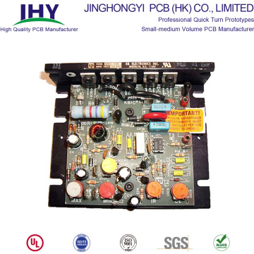
We offer low-volume, Prototype and Production PCB fabrication service, for HDI PCB, rigid PCB, flexible PCB, High Tg boards, etc. All project comes with satisfaction guarantee and on-time delivery.
The attributes of the displayed product
Type
HDI PCB
Layers
8 Layer
Base Material
FR4 Tg170
Dielectric
Prepreg
Board Thickness
1.6mm±10%
Copper Weight
1oz
Surface Finish
ENIG 2U"+Gold Plating 30U"
Minimum trace Width/Spacing
0.1/0.1mm(4/4mils)
Solder Mask Color
Green
Silkscreen Color
White
Min. Hole Size
0.15mm
Via in Pad
Yes
Epoxy Via Plug
Yes
Hole Copper Wall Thickness
25.4um
Controlled Impedance
Yes
Flame Retardant Properties
94 V-0
Application
Industrial Controllers
The Concept
HDI: High Density Interconnection Technology. It is a multilayer board made by a build-up method and a micro-blind buried hole.
Micro-hole: In a PCB, a hole less than 6 mil (150 um) in diameter is called a micro-hole.
Buried Via: buried in the inner layer of the hole, not visible in the finished product, mainly used for the conduction of the inner layer line, can reduce the probability of signal interference, and keep the continuity of the characteristic impedance of the transmission line. Since the buried via does not occupy the surface area of the PCB, more components can be placed on the surface of the PCB.
Blind Via: connecting the surface layer and the inner layer without passing through the full-board via holes.
Key HDI PCB Benefits
The evolution of high-density PCB technology has given engineers greater design freedom and flexibility than ever before. Designers using HDI high density interconnect methods now can place more components on both sides of the raw PCB if desired. In essence, an HDI PCB gives designers more space to work with, while allowing them to place smaller components even closer together. This means that a high-density interconnect PCB ultimately results in faster signal transmission along with enhanced signal quality.
HDI PCB is widely used to reduce the weight and overall dimensions of products, as well as to enhance the electrical performance of the device. The high-density PCB is regularly found in mobile phones, touch-screen devices, laptop computers, digital cameras and 4G network communications. The HDI PCB is also prominently featured in medical devices, as well as various electronic aircraft parts and components. The possibilities for high-density interconnect PCB technology seem almost limitless.
HDI Printed Circuit Boards Structures:
- Suitable for BGA with lower I/O counts
- Fine line, microvia and registration technologies capable of 0.4 mm ball pitch
- Qualified material and surface treatment for Lead-free process
- Excellent mounting stability and reliability
- Copper filled via
Application: Cell phone, UMPC, MP3 Player, PMP, GPS, Memory Card

- Suitable for BGA with smaller ball pitch and higher I/O counts
- Increase routing density in complicated design
- Thin board capabilities
- Lower Dk / Df material enables better signal transmission performance
- Copper filled via
Application: Cell phone, PDA, UMPC, Portable game console, DSC, Camcorder
2+N+2 HDI PCB Structure:

- Every layer via structure maximizes design freedom
- Copper filled via provides better reliability
- Superior electrical characteristics
- Cu bump and metal paste technologies for very thin board
Application: Cell phone, UMPC, MP3, PMP, GPS, Memory card.

Benefits of using HDI Printed Circuit Boards
As consumer demands change, so must technology.
By using HDI technology, designers now have the option to place more components on both sides of the raw PCB.
Multiple via processes, including via in pad and blind via technology, allow designers more PCB real estate to place components that are smaller even closer together.
Decreased component size and pitch allow for more I/O in smaller geometries. This means faster transmission of signals and a significant reduction in signal loss and crossing delays.
HDI Technology PCB Prototype fabrication manufacturer
HDI Technology PCB, one of the fastest growing technologies in PCBs, are now available at JHY PCB whatever PCB Prototyping or Express HDI PCB .HDI Boards contain blind and/or buried vias and often contain microvias of .006 or less in diameter.
Find a HDI PCB Manufacturer and Supplier. Choose Quality HDI PCB Manufacturers, Suppliers, Exporters at pcbjhy.com.Welcome to send your design to us.
Related Keywords
-

PCB Assembly SMT PCB Stencil PCB Stencil Maker

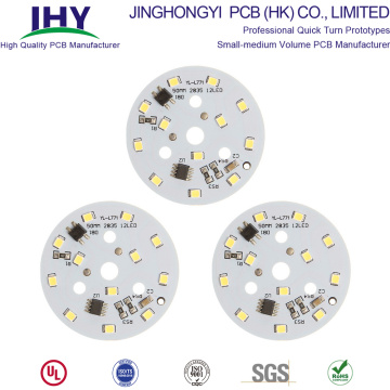
High Quality 24V LED PCB Circuit Board Assembly

Customized Single-sided 12V SMD LED PCB Circuit Board
Related ProductsProduct Categories-
PCB Prototype(97)
-
Quick Turn PCB(33)
-
LED PCB(114)
-
Single Sided PCB(15)
-
Double Sided PCB(60)
-
Multilayer PCB(149)
-
Rigid PCB(22)
-
Flexible PCB(48)
-
Rigid Flex PCB(43)
-
Aluminum PCB(62)
-
Metal Core PCB(50)
-
Thick Copper PCB(106)
-
HDI PCB(61)
-
Impedance Control PCB(27)
-
BGA PCB(11)
-
High TG PCB(32)
-
Fr4 PCB(44)
-
Gold Fingers PCB(29)
-
PCB Application(5)
-
PCB Stencil(56)
-
PCB Assembly Service(67)
-
High Frequency PCB(47)