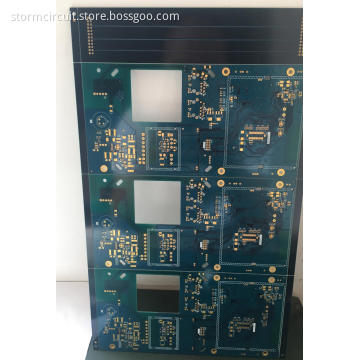

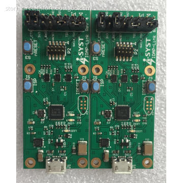
4 layer 0.8mm laser drill PCB
- Payment Type:
- T/T, Paypal, Western Union
- Incoterm:
- FOB, CFR, CIF
- Delivery Time:
- 8 Days
- Transportation:
- Ocean, Land, Air
Your message must be between 20 to 2000 characters
Contact Now| Payment Type: | T/T,Paypal,Western Union |
|---|---|
| Incoterm: | FOB,CFR,CIF |
| Transportation: | Ocean,Land,Air |
In terms of technological processes, these via in pad holes are generally divided into three types, namely blind vias, buried vias, and through vias. The blind holes are located on the top and bottom surfaces of the printed circuit board and have a certain depth. They are used to connect the surface layer circuit and the inner layer circuit below. The depth of the hole usually does not exceed a certain ratio (aperture). A buried hole is a connection hole located in the inner layer of the printed circuit board, which does not extend to the surface of the circuit board. The above two types of holes are located in the inner layer of the circuit board. Before lamination, the through-hole forming process is used to complete the process. In the process of via formation, several inner layers may be overlapped. The third type is called a through-hole. This kind of hole penetrates the entire circuit board and can be used to achieve internal interconnection or as a component positioning hole. Because the through hole is easier to implement in the process and lower cost, it is used by most printed circuit boards instead of the other two through-holes.
PCB features:
1.Layer: 4
2.Material: FR4
3.Thickness:0.8mm
4.Copper: 1OZ
5.Mini hole: 0.075mm
7.Mini width/space: 0.15mm/0.15mm
8.Finish: Immersion Gold

Our manufacturing capability:
Manufacture capability layers: 1-32 layers
Materials: CEM1, CEM3, Rogers, FR-4, high TG FR-4, aluminum base, halogen free
Max board Size: 510*1200mm
Material: RoHS Directive-compliant
PCB thickness: 1.6mm-6.4mm
Out layer copper thickness: 1-6oz
Inner layer copper thickness: 1OZ-12OZ
Max board thickness: 6.0mm
Minimum hole size: 0.150mm
Minimum line width/space: 3/3mil
Min S/M pitch: 0.1mm (4mil)
Plate thickness and aperture ratio: 12:1
Minimum hole copper: 20μm
Hole diameter tolerance (PTH): ±0.075mm (3mil)
Hole diameter tolerance (NPTH): ±0.05mm (2mil)
Hole position deviation: ±0.05mm (2mil)
Outline tolerance: ±0.05mm (2mil)
Surface finish: HASL leadfree, immersion ENIG, chem tin, flash gold, OSP, gold finger, peelable, immersion silver,ENEPIG
Solder mask: green/blue/red/black,purple,white,yellow,transparent
Legend: white/black/yellow
Outline: rout and score/V-cut
E-test: 100%
Top 10 Reasons Why You Should Buy PCBs and PCBAs From Storm Circuit
1.TOP Quality--
It must be the first important key.We always put quality as the first.In PCB industrial,we have over 99% equipments in house. Drilling,Plating,Pressing,AOI (Auto-optical Inspection),Testing,etc.That is why we can guarantee our quality.
2.Shipping On Time even Early
Our Standard lead time for 1-2 layer is 5 working days,Multi-layer 6-8 working days.What is standard? see details. And our Express Service offer 1-2 days for double sided boards,3 days for multilayer boards.
3.High Mix boards
Whatever you need normal FR4,high TG ,Aluminum board,RF board with low Er,heavy copper.large board,high tech board with blind/burried vias.impedence control boards.we can offer such products in quick turn as we have many different material in stock.
4.Technical Support.Free DFM,free file review
Many customers (especially for some designers) are not good at manufacturing process,even they can not generate correct gerber file from their EDA.With much experience in PCB industrial,here are some design tips for you.7*24 online support except our Chinese New Year.
5.StormProto Service
what is stormproto ? see here.You want to cut prototypes cost,that is our stormproto value.With this service,you can save at least 50% cost.
6.Reasonable Price
Our price is NOT cheapest but is the most reasonable cost.You trust us,then we can offer you our best products and service.
7.Fast Response,Fast Shipping
Each enquiry can be replied in 2 hours.2-3 days from us to your door.see shipment.
8.NO MOQ
We do not have any minimum quantity requirements,even -one board for PCB fabrication and assemble.
9.One Stop Service
We not only produce PCB ,but also PCBA and cable assemble .A bare PCB is not what you want,you may need stencil to screen,components to load and cable to connect. Now,you can throw all to us and wait your final product on your desk.
10.Large in-house stock of parts
We have many components stock in house,that is you will save much time and cost on your total project.Especially for any resistors,capacitors

Related Keywords
-

2 layer PCB 1.6mm blue solder HAL

4 layer HDI PCB with 0.1mm holes

Best PCB Prototype Assembly Service
Related ProductsProduct Categories-
Multilayer PCB(61)
-
HDI PCB(26)
-
Rigid-flex PCB(27)
-
Flex PCB(22)
-
MC PCB(21)
-
PCB Assembly(33)
-
ENEPIG PCB(23)
-
RF PCB(23)
-
Microwave PCB(4)
-
Heavy Copper PCB(26)
-
Via In Pad PCB(23)
-
Impedance Control Board(23)
-
Peelable Solder Mask(7)
-
Prototype PCB(47)
-
LED PCB(12)
-
Quick Turn PCB(33)
-
Double-sided PCB(53)
-
10 Layer PCB(5)
-
4 Layer PCB(22)
-
6 Layer PCB(16)