


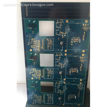
4 layer 1.0mm VIa in Pad PCB
- Payment Type:
- T/T, Paypal, Western Union
- Incoterm:
- FOB, CFR, CIF
- Delivery Time:
- 10 Days
- Transportation:
- Ocean, Land, Air
Quantity:
Your message must be between 20 to 2000 characters
Contact NowBasic Info
Basic Info
| Payment Type: | T/T,Paypal,Western Union |
|---|---|
| Incoterm: | FOB,CFR,CIF |
| Transportation: | Ocean,Land,Air |
Product Description
Product Description
There are numerous benefits of via in pad PCB. It helps to increase density, lessen inductance and use finer pitch packages. In via in pad process, a via is directly placed below the device`s contact pads. This enables greater part density and superior routing. Therefore, via in pad furnishes the considerable board space savings to the PCB designer
PCB features:
1.Layer: 42.Material: FR4
3.Thickness: 1.0mm
4.Copper: 1oz
5.Mini hole: 0.15mm
6.Mini width/space: 0.1mm/0.1mm
7.Finish: Immersion Gold
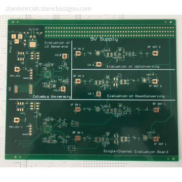
Our manufacturing capability:
Manufacture capability layers: 1-32 layers
Materials: CEM1, CEM3, Teflon, Rogers, FR-4, high TG FR-4, aluminum base, halogen free
Max board Size: 510*1200mm
Material: RoHS Directive-compliant
PCB thickness: 1.6mm-6.4mm
Out layer copper thickness: 1-6oz
Inner layer copper thickness: 1OZ-12OZ
Max board thickness: 6.0mm
Minimum hole size: 0.150mm
Minimum line width/space: 3/3mil
Min S/M pitch: 0.1mm (4mil)
Plate thickness and aperture ratio: 12:1
Minimum hole copper: 20μm
Hole diameter tolerance (PTH): ±0.075mm (3mil)
Hole diameter tolerance (NPTH): ±0.05mm (2mil)
Hole position deviation: ±0.05mm (2mil)
Outline tolerance: ±0.05mm (2mil)
Surface finish: HASL leadfree, immersion ENIG, chem tin, flash gold, OSP, gold finger, peelable, immersion silver,ENEPIG
Solder mask: green/blue/red/black,purple,white,yellow,transparent
Legend: white/black/yellow
Outline: rout and score/V-cut
E-test: 100%

Related Keywords
Related Keywords
You May Also Like
You May Also Like
-

6 layer FR4(TG170) blue ENIG PCB

ENIG 4 Layer PCB with 0.1mm drill holes

PCB Assembly Circuit Boards and Assembly OEM EMS for High Precision Size Products
Related ProductsProduct Categories-
Multilayer PCB(61)
-
HDI PCB(26)
-
Rigid-flex PCB(27)
-
Flex PCB(22)
-
MC PCB(21)
-
PCB Assembly(33)
-
ENEPIG PCB(23)
-
RF PCB(23)
-
Microwave PCB(4)
-
Heavy Copper PCB(26)
-
Via In Pad PCB(23)
-
Impedance Control Board(23)
-
Peelable Solder Mask(7)
-
Prototype PCB(47)
-
LED PCB(12)
-
Quick Turn PCB(33)
-
Double-sided PCB(53)
-
10 Layer PCB(5)
-
4 Layer PCB(22)
-
6 Layer PCB(16)


