

Via in pad PCB Prototype Fabrication
Your message must be between 20 to 2000 characters
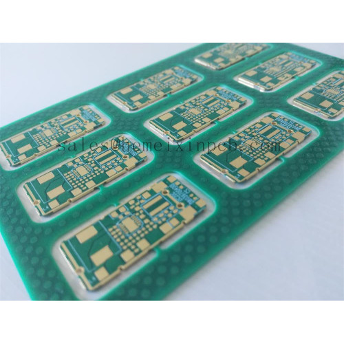
Contact NowIn PCB design, via refers to a pad with a plated hole that connects copper tracks from one layer of the board to other layer(s). High Density Multilayer PCBs may have what is normally referred to as micro vias micro used as blind vias, which are visible only on one surface, or buried vias, which are visible on neither The advent and extensive use of finer pitch devices and requirements for smaller size PCBs creates new challenges. An exciting solution to these challenges uses a recent, but common PCB manufacturing technology with self-descriptive name, [Via In Pad".
HemeixinPCB has created the option of checking the required impedance on the customer's circuit board, so as to modify the circuit board, or the tracks and the layer structure if necessary. The impedance is largely determined by the track geometry, the structure of the layers and the dielectric constant (Er) of the materials used.
After making the circuit board, the impedances are checked and recorded. The results of the measurements are available on request at any time.


Related Keywords
-

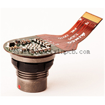
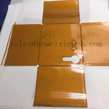
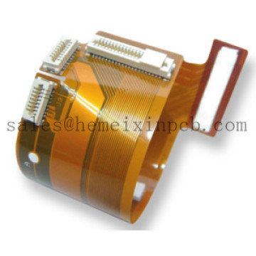
Flex Printed Circuits assembly

Prototype Kapton Flexible circuits

Prototype Polyimide Flexible pcb
Related ProductsProduct Categories-
Microvia PCB(1)
-
Microwave PCB(13)
-
Heavy Copper PCB(4)
-
Metal Core PCB(10)
-
Turn-key PCB Assembly(19)
- Circuit Board Assembly(1)
- PCB Assembly(1)
- Rigid PCB Assembly(1)
- PCB Board Assembly(1)
- Circuit Card Assembly(1)
- SMT PCB(1)
- PCB Turnkey(1)
- Pcb Assembly Manufacturer(1)
- Pcb Assembly Quote(1)
- Pcb Assy(1)
- Electro Mechanical Assembly(1)
- Electronic Circuit Board Assembly(1)
- Pcb Manufacturing And Assembly(1)
- Electronic PCB Contract Manufacturing(1)
- Electronic PCB Assembly(1)
- Microelectronic Assembly(1)
- RF PCB Assembly(1)
- Wireless PCB Assembly(1)
- Turnkey PCB Assembly(1)
-
Rigid Flex PCB Assembly(12)
- Rigid Flexible Circuits Assembly(1)
- Rigid-flex Circuits Assembly(1)
- Flex-rigid Circuits Assembly(1)
- Flex-rigid Pcb Assembly(1)
- Rigid Flexible PCB Assembly(1)
- Rigid Flex Circuit Assembly(1)
- Rigid Flex Circuits Assembly(1)
- Flex Rigid PCB Assembly(1)
- Semiflex Pcb Assembly(1)
- Starr Flex PCB Assembly(1)
- Rigiflex Pcb Assembly(1)
- Rigid-Flexible PCB Assembly(1)
-
PCB Prototype Assembly(2)
-
Flexible Circuits Assembly(15)
- Flex Printed Circuits Assembly(1)
- Multilayer Flexible PCB Assembly(1)
- Microvia Flex Circuit Assembly(1)
- Flat Flex PCB Assembly(1)
- Flex Cable Circuit Board Assembly(1)
- Flexible Circuitry Assembly(1)
- HDI Flexible PCB Assembly(1)
- Microvia Flex PCB Assembly(1)
- HDI Flexible Circuit Assembly(1)
- Kapton PCB Assembly(1)
- Polyimide Pcb Assembly(1)
- Kapton Flexible PCB Assembly(1)
- Polyimide Flexible Circuit Assembly(1)
- Flex PCB Assembly(1)
- Flexible Printed Circuit Board Assembly(1)
-
PCB Assembly(9)
-
Flexible Circuits(19)
- Flex Printed Circuits(1)
- Multilayer Flexible PCB(1)
- Flexible Heater(1)
- Flat Flex PCB(1)
- Flex Cable Circuit(1)
- Flexible Circuitry(1)
- HDI Multilayer Flexible PCB(1)
- Microvia Flex PCB(1)
- HDI Flexible Circuit(1)
- Microvia Flex Circuit(1)
- Flex Pcb Manufacturer(1)
- Flex Pcb Fabrication(1)
- Flexible Circuit Board(1)
- Flex PCB(1)
- Kapton PCB(1)
- Polyimide Pcb(1)
- Kapton Flexible PCB(1)
- Polyimide Flexible Circuit(1)
- Flexi Circuits(1)
-
Rigid Flex PCB(11)

