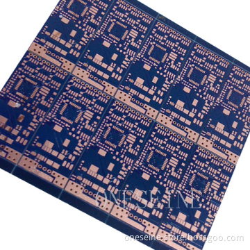

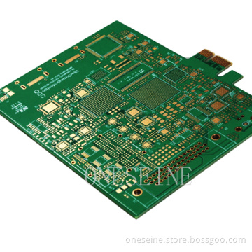
6 multilayer pcb board with Min line width 0.13mm impedance control 50Ohms
- Payment Type:
- T/T, Paypal, Western Union
- Incoterm:
- FOB, CIF
- Min. Order:
- 1 Piece/Pieces
- Min. Order:
- 1 Piece/Pieces
- Delivery Time:
- 5 Days
- Transportation:
- Air
Your message must be between 20 to 2000 characters
Contact Now| Payment Type: | T/T,Paypal,Western Union |
|---|---|
| Incoterm: | FOB,CIF |
| Transportation: | Air |
6 multilayer pcb board with Min line width 0.13mm impedance control 50Ohms
|
Material:FR4 |
Soldermask:Green |
|
Molde Number:ONE-5 |
Silkscreen:White |
|
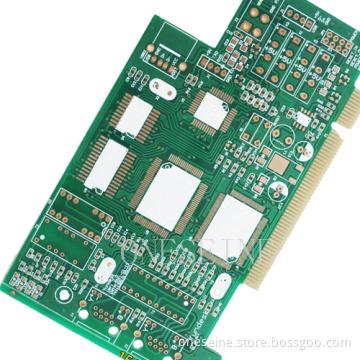
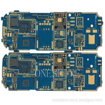
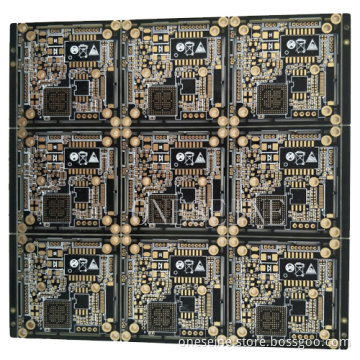
Layer:6 |
Panel Size:185*55mm |
|
Board Thickness:0.8mm |
Package Details: Inner:Vacuum-packed Bubble bag With Foam Outer:Carton Box |
|
Min Line Space:4Mil |
|
|
Min Line Width:4Mil |
|
|
Min Hole Size:10Mil |
|
|
Finished Surface:ENIG |
Special requirement: Min Line width 0.13mm Impedance Control 50Ohms Provide Shipment Report |
|
Finished Copper:1oz |
|
|
Delivery Time:8 Days |
Defined impedance 6 multilayer pcb board is: a good laminated structure will be able to play on the printed circuit board characteristic impedance control, the traces can be formed easily controlled and predictable transmission line structure is called impedance plate.
Current common characteristic impedance is divided into: single-ended (line) impedance differential (fixed) impedance coplanar impedance.
Single-ended (wire) Impedance: English single ended impedance, refers to a single signal line measured impedance.
Difference (Fixed) Impedance: English differential impedance, differential drive means to the test in two monospaced equally spaced transmission line impedance.
Q1: How do you make sure the quality of the PCBs?
A1.Because all in 100% Testing,including Flying Probe Test,E-test or AOI.
Q2: Can I get the best price?
A2.Yes,we will try our best to quote the better price to you,and also try our best to support our customer.
Q3: What is the lead time?
A3.For multilayer sample,if the board not very difficult,needs 1-4 working days;For mass production,needs 8-10 working days,depands on the board and quantity.
Q4: What files should we offer?
A4.PCB Gerber files ,protel,powerpcb,Autocad,etc;BOM list for PCB assembly;Send us your sample PCB or PCBA;OEM is acceptable
|
Specifications |
Technology |
Notes |
|
Number of Layers |
1-28 Layers |
|
|
Board Materials |
FR4 (Tg 135, 145, 170,180)
Taconic(TLY-5,TLY-3,TLY-8 etc.) |
We keep these materials in stock. If you need a material that is not listed here, please contact us and we can order it for you. |
|
Final PCB Thickness |
2 Layer – Min .005" Max .250" |
|
|
Core Thickness |
Min .0025" |
|
|
Maximum PCB Size |
2 Layer 20" x 28" |
|
|
Minimum Conductor Space |
0.003" |
|
|
Minimum Conductor Width |
0.003" |
|
|
Minimum Drill Hole Size |
0.006" |
|
Advantage
1. PCB factory directly
2. PCB Have the comprehensive quality control system
3. PCB good price
4. PCB quick turn delivery time from 48hours.
5. PCB certification(ISO/UL E354810/RoHS)
6. 12 years experience in exporting service
7. PCB is no MOQ/MOV.
8. PCB is high quality.Strict through theAOI(Automated Optical Inspection),QA/QC,fly porbe ,Etesting

Related Keywords