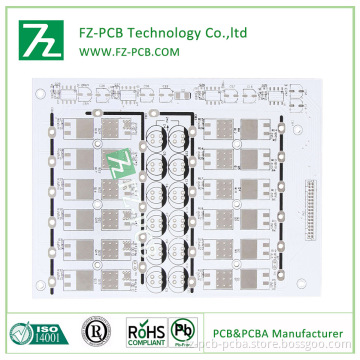
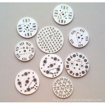
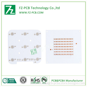
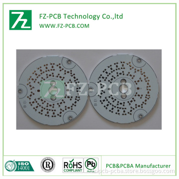
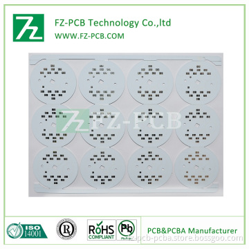
Double Side Immersion Gold LED PCB (PCB LED)
- Payment Type:
- T/T, Paypal, Western Union
Quantity:
Your message must be between 20 to 2000 characters
Contact NowBasic Info
Basic Info
| Place of Origin: | Shenzhen, China |
|---|---|
| Payment Type: | T/T, Paypal, Western Union |
Product Description
Product Description
Testing Procedures For PCB Board:
* Flying probe
* Impedance control
* Solder-ability detection
* Digital metallograghic microscope
* AOI (Automated Optical Inspection)
How to get a quote?
Pls send gerber file with these format: . PCB /. P-CAD /. DXP /. CAD /. Gerber
A) Base material: FR4/ AL/ FPC/ CEM-1/ CEM-3/ 94v0/ Rogers
B) Board thickness: 1.6mm-3.2mm/ 0.3mm-1.2mm
C) Copper thickness: Hoz/ 1oz/ 2oz/ 3oz/ 4oz, ect
D) Surface treatment: HASL/ ENIG/ LF-HAL/ Immersion Tin/ Immersion Sin/ OSP
E) color of solder mask and silkscreen: Green/White/Black/Red/Blue/Yellow
F) Quantity and board size
Delivery Time for PCB board:
1) PCB production time: Sample: 4-5 days / production: Within 9 days
2) Component purchase: 2 days if all components is available in our domestic market.
PCB Assembly: Samples: Within 5 days / mass production: Within 9 days
Shipping Method and Payment terms:
1. By DHL, UPS, FedEx, TNT using clients account.
2. We suggest you using our DHL, UPS, FedEx, TNT forwarder.
3. By EMS (Usually for Russia Clients), price is high.
4. By sea for mass quantity according to customer's requirement.
5. By customer's Forwarder
6. By Paypal, T/T, West Union, etc.
| Files | Gerber, Protel, Powerpcb, Autocad, Orcad, etc |
| Material | FR-4, Hi-Tg FR-4, Lead free Materials (RoHS Compliant) , FR1, CEM-3, CEM-1, Aluminium, High frequency Material (Rogers, Teflon, Taconic), Polymide. |
| Layer No. | 1 - 20 Layers |
| Board thickness | 0.0075"(0.2mm)-0.125"(3.2mm) |
| Board Thickness Tolerance | ±10% |
| Copper thickness | 0.3OZ - 6OZ |
| Impedance Control | ±10% |
| Warp and Twist | ≤0.075% |
| Peel Strength | ≥61B/in(≥107g/mm) |
| Min Trace Width (a) | 3mil |
| Min Space Width (b) | 3mil |
| Min Annular Ring | 0.004"(0.1mm) |
| SMD Pitch (a) | 0.012"(0.3mm) |
| pcb with green solder mask and LF-FREE surface finishing BGA Pitch (b) | 0.027"(0.675mm) |
| Register tolerance | 0.05mm |
| Min Solder Mask Dam (a) | 0.005"(0.125mm) |
| Solder mask Clearance (b) | 0.005"(0.125mm) |
| Min SMT Pad spacing (c) | 0.004"(0.1mm) |
| Solder Mask Thickness | 0.0007"(0.018mm) |
| Hole size | 0.008"(0.20mm)-- 0.257"(6.5mm) |
| Hole Size Tol (+/-) | ±0.003"(±0.0762mm) |
| Max PTH Aspect Ratio | 10:1 |
| Hole Registration | 0.003"(0.075mm) |
| HASL | 2.5um |
| Lead free HASL | 2.5um |
| Immersion Gold | Nickel 3-7um Au:1-3u'' |
| OSP | 0.2-0.5um |
| Panel Outline Tol (+/-) | ±0.004''(±0.1mm) |
| Beveling | 30°45° |
| V-cut | 15° 30° 45° 60° |
| Surface finish | HAL, HASL Lead Free, Immersion gold, Gold plating, Gold finger, immersion silver, immersion Tin, OSP, Carbon ink, |
| Certificate | ROHS ISO9001 TS16949 SGS UL |
| Special requirements | Buried&blind vias, Impedance control, via plug, BGA soldering and gold finger |

Related Keywords
Related Keywords
You May Also Like
You May Also Like