Double Side Electronics PCB
- Payment Type:
- T/T, Paypal, Western Union
Quantity:
Your message must be between 20 to 2000 characters
Contact NowBasic Info
Basic Info
| Place of Origin: | Shenzhen, China |
|---|---|
| Payment Type: | T/T, Paypal, Western Union |
Product Description
Product Description
One-stop PCB assembly service, 1~16 Layers PCB, 1~8 layers PCBA, PCB design, PCB layout, PCB manufacturing, PCB Assemblies, components sourcing, PCBA Function Test, design solution.
All conform to RoHS/UL, ISO9001: 2008 & ISO/TS16949: 2009, ISO14001:2004
Testing Procedures For PCB Board:
* Visual Inspection
* Flying probe
* Impedance control
* Solder-ability detection
* Digital metallograghic microscope
* AOI (Automated Optical Inspection)
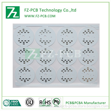
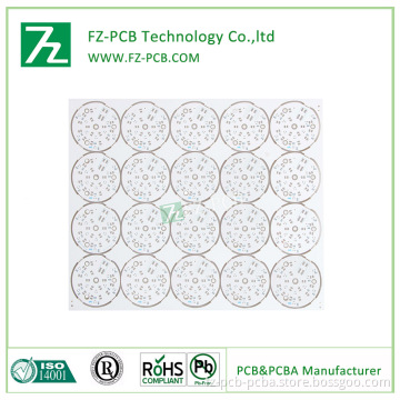
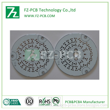
FR-4 PCB Show


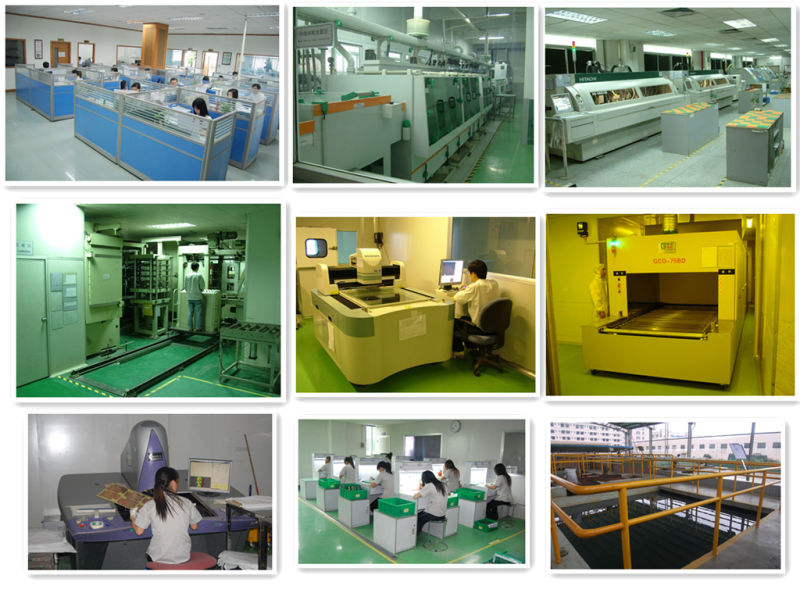
Factory glance
All conform to RoHS/UL, ISO9001: 2008 & ISO/TS16949: 2009, ISO14001:2004
Testing Procedures For PCB Board:
* Visual Inspection
* Flying probe
* Impedance control
* Solder-ability detection
* Digital metallograghic microscope
* AOI (Automated Optical Inspection)
How to get a quote?
Pls send gerber file with these formats: .PCB / .P-CAD / .DXP / .CAD / .Gerber
a) Base material: FR4/ AL/ FPC/ CEM-1/ CEM-3/ 94v0/ Rogers
b) Board thickness: 1.6mm-3.2mm/ 0.3mm-1.2mm
c) Copper thickness: Hoz/ 1oz/ 2oz/ 3oz/ 4oz, ect
d) Surface treatment: HASL/ ENIG/ LF-HAL/ Immersion Tin/ Immersion Sin/ OSP
e) color of solder mask and silkscreen: Green/White/Black/Red/Blue/Yellow
f) Quantity and board size
FR-4 PCB Show


Factory glance

| Files | Gerber, Protel, Powerpcb, Autocad, Orcad, etc |
| Material | FR-4, Hi-Tg FR-4, Lead free Materials (RoHS Compliant) , FR1, CEM-3, CEM-1, Aluminium, High frequency Material (Rogers, Teflon, Taconic), Polymide. |
| Layer No. | 1 - 16Layers |
| Board thickness | 0.0075"(0.2mm)-0.200"(5.0mm) |
| Board Thickness Tolerance | ±10% |
| Copper thickness | 0.3OZ - 6OZ |
| Impedance Control | ±10% |
| Warp and Twist | ≤0.075% |
| Peel Strength | ≥61B/in(≥107g/mm) |
| Min Trace Width (a) | 3mil |
| Min Space Width (b) | 3mil |
| Min Annular Ring | 0.004"(0.1mm) |
| SMD Pitch (a) | 0.012"(0.3mm) |
| pcb with green solder mask and LF-FREE surface finishing BGA Pitch (b) | 0.027"(0.675mm) |
| Register tolerance | 0.05mm |
| Min Solder Mask Dam (a) | 0.005"(0.125mm) |
| Solder mask Clearance (b) | 0.005"(0.125mm) |
| Min SMT Pad spacing (c) | 0.004"(0.1mm) |
| Solder Mask Thickness | 0.0007"(0.018mm) |
| Hole size | 0.008"(0.20mm)-- 0.257"(6.5mm) |
| Hole Size Tol (+/-) | ±0.003"(±0.0762mm) |
| Max PTH Aspect Ratio | 10:1 |
| Hole Registration | 0.003"(0.075mm) |
| HASL | 2.5um |
| Lead free HASL | 2.5um |
| Immersion Gold | Nickel 3-7um Au:1-3u'' |
| OSP | 0.2-0.5um |
| Panel Outline Tol (+/-) | ±0.004''(±0.1mm) |
| Beveling | 30°45° |
| V-cut | 15° 30° 45° 60° |
| Surface finish | HAL, HASL Lead Free, Immersion gold, Gold plating, Gold finger, immersion silver, immersion Tin, OSP, Carbon ink, |
| Certificate | ROHS ISO9001 TS16949 SGS UL |
| Special requirements | Buried&blind vias, Impedance control, via plug, BGA soldering and gold finger |

Related Keywords
Related Keywords
You May Also Like
You May Also Like