
Double Side FR4 Green ENIG Immersion Gold Custom Printed Ci
- Min. Order:
- 1
- Min. Order:
- 1
- Delivery Time:
- 30 Days
Quantity:
Your message must be between 20 to 2000 characters
Contact NowBasic Info
Basic Info
| Place of Origin: | China |
|---|
Product Description
Product Description
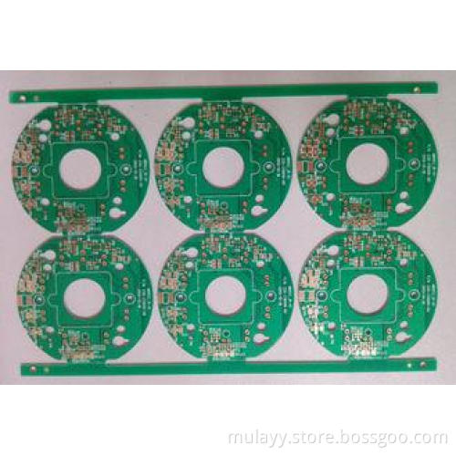
Double Side FR4 Green ENIG Immersion Gold Custom Printed Circuit Board PCB
| PRODUCT’S DETAILS | |
| Raw Material | FR-4 |
| Layer Count | 2-Layer |
| Board Thickness | 1.6mm |
| Copper Thickness | 2.0oz |
| Surface Finish | ENIG(Electroless Nickel Immersion Gold) |
| Solder Mask | Blue |
| Silkscreen | White |
| Min. Trace Width/Spacing | 0.075/0.075mm |
| Min. Hole Size | 0.25mm |
| Hole Wall Copper Thickness | ≥20μm |
| Measurement | 300×400mm |
| Packaging | Inner: Vacuum-packed in soft plastic bales Outer: Cardboard Cartons with double straps |
| Application | Communication,automobile,cell,computer,medical |
| Advantage | Competitive Price,Fast Delivery,OEM&ODM,Free Samples, |
| Special Requirements | Buried And Blind Via, Impedance Control, Via Plug, BGA Soldering And Gold Finger Are Acceptable |
| Certification | UL,ISO9001:2008,ROHS,REACH,SGS,HALOGEN-FREE |
| PRODUCTION CAPABILITY OF PCB | ||
PROCESS Engineer | ITEMS Item | PRODUCTION CAPABILITY Manufacturing Capability |
| Laminate | Type | FR-1,FR-5,FR-4 High-Tg,ROGERS,ISOLA,ITEQ, ALUMINUM,CEM-1,CEM-3,TACONIC,ARLON,TEFLON |
| Thickness | 0.2~3.2mm | |
| Production Type | Layer Count | 2L-16L |
| Surface Treatment | HAL,Gold Plating,Immersion Gold,OSP, Immersion Silver,Immersion Tin,Lead Free HAL | |
| Cut Lamination | Max. Working Panel size | 1000×1200mm |
| Inner Layer | Internal Core Thickness | 0.1~2.0mm |
| Internal width/spacing | Min: 4/4mil | |
| Internal Copper Thickness | 1.0~3.0oz | |
| Dimension | Board Thickness Tolerance | ±10% |
| Interlayer Alignment | ±3mil | |
| Drilling | Manufacture Panel Size | Max: 650×560mm |
| Drilling Diameter | ≧0.25mm | |
| Hole Diameter Tolerance | ±0.05mm | |
| Hole Position Tolerance | ±0.076mm | |
| Min.Annular Ring | 0.05mm | |
| PTH+Panel Plating | Hole Wall copper Thickness | ≧20um |
| Uniformity | ≧90% | |
| Outer Layer | Track Width | Min: 0.08mm |
| Track Spacing | Min: 0.08mm | |
| Pattern Plating | Finished Copper Thickness | 1oz~3oz |
| EING/Flash Gold | Nickel Thickness | 2.5um~5.0um |
| Gold Thickness | 0.03~0.05um | |
| Solder Mask | Thickness | 15~35um |
| Solder Mask Bridge | 3mil | |
| Legend | Line width/Line spacing | 6/6mil |
| Gold Finger | Nickel Thickness | ≧120u〞 |
| Gold Thickness | 1~50u〞 | |
| Hot Air Level | Tin Thickness | 100~300u〞 |
| Routing | Tolerance of Dimension | ±0.1mm |
| Slot Size | Min:0.4mm | |
| Cutter Diameter | 0.8~2.4mm | |
| Punching | Outline Tolerance | ±0.1mm |
| Slot Size | Min:0.5mm | |
| V-CUT | V-CUT Dimension | Min:60mm |
| Angle | 15°30°45° | |
| Remain Thickness Tolerance | ±0.1mm | |
| Beveling | Beveling Dimension | 30~300mm |
| Test | Testing Voltage | 250V |
| Max.Dimension | 540×400mm | |
| Impedance Control | Tolerance | ±10% |
| Aspect Ration | 12:1 | |
| Laser Drilling Size | 4mil(0.1mm) | |
| Special Requirements | Buried And Blind Via, Impedance Control, Via Plug, BGA Soldering and Gold Finger Are Acceptable | |
| OEM&ODM Service | Yes | |
Quick Details
- One of the largest PCB(Printed Circuit Board) manufacturers in China with over 500 staff.
- One of the professional PCB manufacturers in China with 20 years’ experience.
- Certifications of ISO9001:2008,UL,CE,ROHS,REACH,HALOGEN-FREE is meet.
- Good quality with competitive price for all kinds of PCB manufactured by SYF.
- One-stop service of PCB with assembly is supplied to our customers.
- Best service with quick response is always provided for our customers.
- All kinds of surface finish is accepted,such as ENIG,OSP.Immersion Silver,Immersion Tin, Immersion Gold, Lead-free HASL,HAL.
- Advanced production equipment imported from Japan and Germany,such as PCB Lamination Machine, CNC drilling machine,Auto-PTH line, AOI(Automatic Optic Inspection),Probe Flying Machine and so on.
- BGA,Blind&Buried Vias and Impedence Control is accepted.


You May Also Like
You May Also Like

