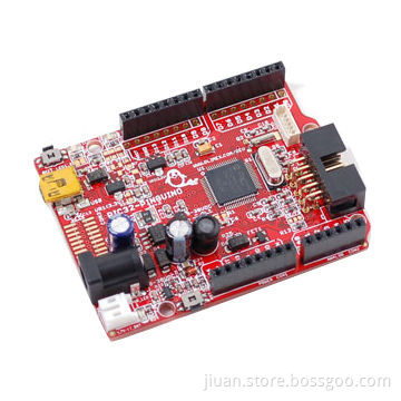
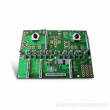
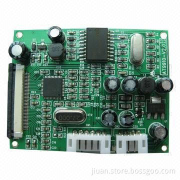
Competitive Price, PCBA/PCB Assembly with High Standard SMT /DIP
- Payment Type:
- T/T in Advance, L/C at Sight, PayPal, Western Unio
Quantity:
Your message must be between 20 to 2000 characters
Contact NowBasic Info
Basic Info
| Payment Type: | T/T in Advance, L/C at Sight, PayPal, Western Unio |
|---|
Product Description
Product Description
- Board thickness: 1.6mm
- Copper thickness: 1oz
- HASL-LF surface finishing
- Green solder mask and white legend
- With UL and RoHS marks
- Fast prototype and mass production for PCB assembly as per buyers' requirement
- Component sourcing, PCB reverse engineering and PIC decoding are available
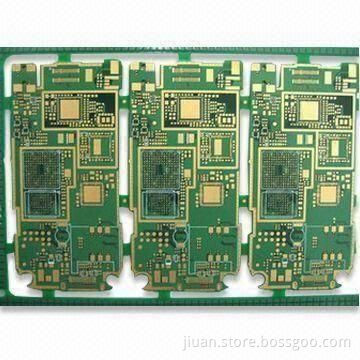
- Maximum layers count for rigid PCB: 1-12
- PCB board thickness: 14-175 mils
- Drill to metal: 7 mils
- Hole size: 6 mils
- Inner layer registration: 3 mils
- Line width and space inner/outer: 3/3 mils (minimum)
- Aspect ratio:
- Minimum solder mask dam: 2.5 mils
- Controlled impedance: ±8%
- Maximum internal copper weight: 3oz
- Advanced technology: blind/buried via, HDI micro via
- Surface treatment: ENIG, OSP, immersion silver/tin, lead-free HASL
- Materials: FR4, high Tg epoxy, halogen-free
- Lead-time: 5-20 days (depends on QTY, production status and more)
- Computers, communications, test and control systems, medical equipment and more
- Minimum solder mask dam: 2.5 mils
Related Keywords
Related Keywords
You May Also Like
You May Also Like
-

Multilayer PCBs with gold plating finish

Competitive Price, PCBA/PCB Assembly with High Standard SMT /DIP

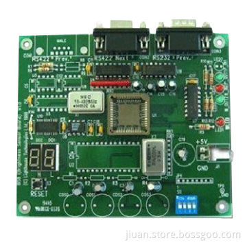
PCB Prototype and Mass Assembly Services, Rigid PCB Assembly

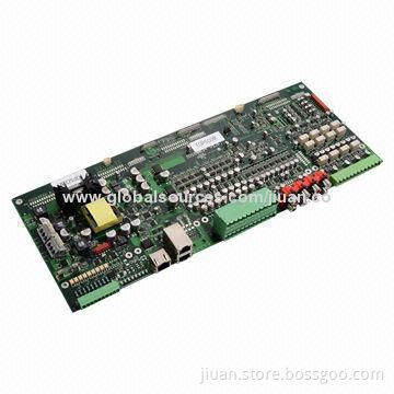
PCB Assembly, OEM/ODM Services are Provided
China PCB Assembly, OEM/EMS Manufacturer for Medical Electronic
Related ProductsProduct Categories-
PCB assemblies(232)
-
Multilayer PCBs(3)
-
Contract manufacturing services(37)
-
Double-sided PCBs(1)
-
Electronic products OEM & ODM services(11)
-
High-density multilayer PCBs(1)
-
Telecom products OEM & ODM services(8)
-
Single-sided PCBs(11)
-
Aluminum PCBs(2)
-
Security products OEM & ODM services(2)
-
FR-4 PCBs(4)
-
Intelligent controller boards(4)
-
Flexible PCBs(1)
-
Medical & health products OEM & ODM services(2)
-
OSP PCBs(1)
-
Rigid-flex PCBs(1)
-
PCB design services(1)