Wonderful PCB (HK) limited
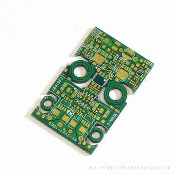
Single-sided Flexible PCB, Flex Printed Circuit Board, Used for HDI Electronic Products
  • Single-sided Flexible PCB, Flex Printed Circuit Board, Used for HDI Electronic Products
Single-sided Flexible PCB, Flex Printed Circuit Board, Used for HDI Electronic Products

Single-sided Flexible PCB, Flex Printed Circuit Board, Used for HDI Electronic Products

Payment Type:
Telegraphic Transfer in Advance (Advance TT, T/T)
Quantity:

Your message must be between 20 to 2000 characters

Contact Now
Basic Info
Basic Info
Payment Type: Telegraphic Transfer in Advance (Advance TT, T/T)
Product Description
Product Description
  • Flex printed circuit board used for HDI electronicproducts
  • UL/SGS/RoHS approvals
  • Key specifications:
    • Used for LCD, mobile phones and other military/civilproducts
    • Materials: FR4 with Hi-TG
    • Surface finish: HAL
    • Copper thickness: 0.3 to 14oz
    • Layer: 1 to 6 layers
  • Application: digital electronic materials, power and securityproducts
  • Our fabrication capacity for PCB:
    • Layer counts: 1 to 28
    • Board finished thickness: 0.21 to 7.0mm
    • Material: FR-4, CEM-1, CEM-3, high TG, FR4 halogen free,rogers
    • Max. finished board size: 23 x 25mil
    • Min. drilled hole size: 3mil (0.075mm)
    • Min. line width: 3mil (0.075mm)
    • Min. line spacing: 3mil (0.075mm)
    • Surface finish/treatment: HASL/HASL lead free, HAL, chemicaltin, chemical gold, immersion silver/gold, OSP, gold plating
    • Copper thickness: 0.5 to 7.0 OZ
    • Solder mask color: green/yellow/black/white/red/blue
    • Copper thickness in hole: >25.0um (>1mil)
    • Inner packing: vacuum packing/plastic bag
    • Outer packing: standard carton packing
    • Shape tolerance: ±0.13
    • Hole tolerance: PTH: ±0.076, NPTH: ±0.05
    • Certificate: UL, ISO 9001:2000, ISO 14001
    • Special requirements: buried and blind vias + controlledimpedance + BGA
    • Profiling: punching, routing, V-CUT, beveling
    • OEM services for all sorts of printed circuit board assembly aswell as electronic encased products
  • Used for LCD, mobile phones and other military/civilproducts
  • Materials: FR4 with Hi-TG
  • Surface finish: HAL
  • Copper thickness: 0.3 to 14oz
  • Layer: 1 to 6 layers
  • Layer counts: 1 to 28
  • Board finished thickness: 0.21 to 7.0mm
  • Material: FR-4, CEM-1, CEM-3, high TG, FR4 halogen free,rogers
  • Max. finished board size: 23 x 25mil
  • Min. drilled hole size: 3mil (0.075mm)
  • Min. line width: 3mil (0.075mm)
  • Min. line spacing: 3mil (0.075mm)
  • Surface finish/treatment: HASL/HASL lead free, HAL, chemicaltin, chemical gold, immersion silver/gold, OSP, gold plating
  • Copper thickness: 0.5 to 7.0 OZ
  • Solder mask color: green/yellow/black/white/red/blue
  • Copper thickness in hole: >25.0um (>1mil)
  • Inner packing: vacuum packing/plastic bag
  • Outer packing: standard carton packing
  • Shape tolerance: ±0.13
  • Hole tolerance: PTH: ±0.076, NPTH: ±0.05
  • Certificate: UL, ISO 9001:2000, ISO 14001
  • Special requirements: buried and blind vias + controlledimpedance + BGA
  • Profiling: punching, routing, V-CUT, beveling
  • OEM services for all sorts of printed circuit board assembly aswell as electronic encased products
  • Send your message to this supplier

    • Ms.  Shengwen

    • Enter between 20 to 4,000 characters.

    Related Keywords

    Related Keywords