
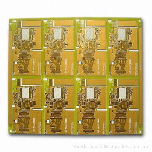
Multilayer PCB, Prototype Used for Camera, with 0.2mm to 7.0mm Board Finish Thickness
- Payment Type:
- Telegraphic Transfer in Advance (Advance TT, T/T)
Your message must be between 20 to 2000 characters
Contact Now| Payment Type: | Telegraphic Transfer in Advance (Advance TT, T/T) |
|---|


Related Keywords
-

Communication Board with Immersion Gold and Gold Finger Surface Finish

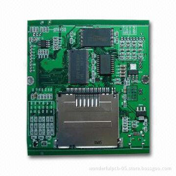
PCBA, Applied to DVD/CD Players with 3mil Minimum Drilled Hole Size

Mobile HDI PCB with 0.5 to 7.0oz Copper Thickness and 1 to 28 Layers

Electronic Circuit, Widely Used for Customer Electronics, Punching, and Routing Profiling

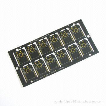
High Quality Multilayer PCB with 4mil Line Width and 0.3mm Minimum Hole Size
Related Products-
Multilayer PCB with Blind and Buried Vias, 0.2 to 7.0mm Thickness, Used to Motherboard
-

PCB Board with Red Solder Mask, Used for MP3, Radio with 1 to 28-layer, Chain PCB Supplier
-

Multilayer PCB with 0.5 to 7.0oz Copper Thickness, Green Solder Mask and ENIG Surface Finish
-

Aluminum PCB with Copper Thickness of 1oz and Single Layer
-
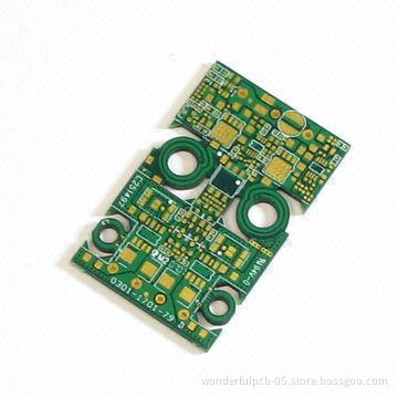
Multilayer PCB with 0.5 to 7.0oz Copper Thickness, 1 to 28 Layers, Blind and Buried Hole Capability
Product Categories-
Multilayer PCBs(114)
-
Double-sided PCBs(89)
-
PCB assemblies(85)
-
High-density multilayer PCBs(68)
-
Aluminum PCBs(62)
-
Flexible PCBs(63)
-
Single-sided PCBs(43)
-
Rigid-flex PCBs(25)
-
Single-sided flexible PCBs(20)
-
Multilayer flexible PCBs(15)
-
Quick-turnaround PCBs(14)
-
PCB laminates(15)
-
PCB design services(10)
-
Split flexible PCBs(9)
-
Double-sided flexible PCBs(6)
-
Double access flexible PCBs(6)
-
Laptop motherboards(5)
-
Immersion gold PCBs(5)
-
Lead free HAL PCBs(5)
-
PCB connectors(3)
-
Immersion silver PCBs(3)
-
Contract manufacturing services(3)
-
PCB terminal blocks(1)


