Wonderful PCB (HK) limited
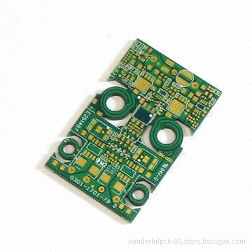
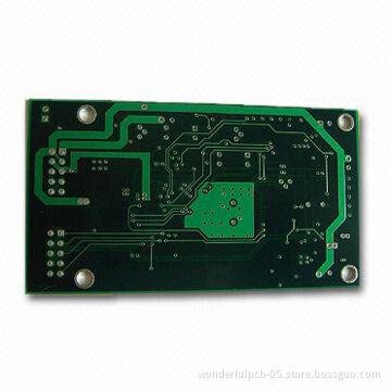
Multi-layer Electronic PCB with 2.4mm Board Thickness, 2oz Copper, HAL Lead-free and GBL Peelable
  • Multi-layer Electronic PCB with 2.4mm Board Thickness, 2oz Copper, HAL Lead-free and GBL Peelable
Multi-layer Electronic PCB with 2.4mm Board Thickness, 2oz Copper, HAL Lead-free and GBL Peelable

Multi-layer Electronic PCB with 2.4mm Board Thickness, 2oz Copper, HAL Lead-free and GBL Peelable

Payment Type:
Telegraphic Transfer in Advance (Advance TT, T/T)
Quantity:

Your message must be between 20 to 2000 characters

Contact Now
Basic Info
Basic Info
Payment Type: Telegraphic Transfer in Advance (Advance TT, T/T)
Product Description
Product Description
  • Copper thickness: 2oz
  • Board thickness: 2.4mm
  • Minimum hole size: 0.26mm
  • Minimum line width/space: 0.24mm/0.16mm ENIG
  • Reference-our production capability for rigid PCB:
    • Layers: 1 to 28
    • Board finishing thickness: 0.21 to 7.0mm
  • Materials: FR-4, CEM-1, CEM-3, high TG, FR4 halogen free andRogers
  • Maximum finishing board dimensions: 23 x 25 (580 x 900mm)
  • Minimum drilled hole size: 3 mils (0.075mm)
  • Minimum line width: 3 mils (0.075mm)
  • Minimum line spacing: 3 mils (0.075mm)
  • Surface finishing/treatment: HASL/HASL lead-free, HAL, chemicaltin, chemical gold, immersion silver/gold, OSP and goldplating
  • Copper thickness: 0.5 to 7.0oz
  • Solder mask color: green/yellow/black/white/red/blue
  • Copper thickness in hole: >25.0um (>1 mil)
  • Packaging:
    • Inner packaging: vacuum packing/plastic bag
    • Outer packaging: standard carton packing
  • Shape tolerance: ±0.13
    • Hole tolerance PTH: ±0.076
    • NPTH: ±0.05
  • Special requirements:
    • Buried and blind vias + controlled impedance + BGA
    • Profiling: punching, routing, v-cut and beveling
    • Provides OEM services to all sorts of printed circuit boardassembly as well as electronic encased products
  • All trademarks shown here are for reference purposesonly. They are the property of their respective owners, and we arenot authorized to sell items bearing such trademarks.
  • Layers: 1 to 28
  • Board finishing thickness: 0.21 to 7.0mm
  • Inner packaging: vacuum packing/plastic bag
  • Outer packaging: standard carton packing
  • Hole tolerance PTH: ±0.076
  • NPTH: ±0.05
  • Buried and blind vias + controlled impedance + BGA
  • Profiling: punching, routing, v-cut and beveling
  • Provides OEM services to all sorts of printed circuit boardassembly as well as electronic encased products
  • Send your message to this supplier

    • Ms.  Shengwen

    • Enter between 20 to 4,000 characters.

    Related Keywords

    Related Keywords