
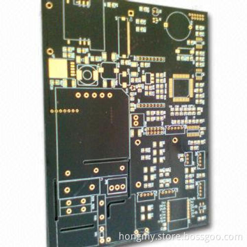
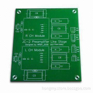
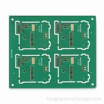
6-layer PCB with Immersion Gold Surface Finish and 2oz Outer Layer Copper Thickness
- Payment Type:
- T/T, Paypal, Western Union
Your message must be between 20 to 2000 characters
Contact Now| Payment Type: | T/T, Paypal,Western Union |
|---|
- Number of layers: six
- Base material: FR4
- Finished board thickness: 1.6mm
- Copper thickness:
- Outer layer: 2oz
- Inner layer: 1oz
- Minimum hole size: 0.11mm
- Minimum line width: 0.075mm
- Minimum line spacing: 0.1mm
- Surface finish: immersion gold
- We offer a wide range of PCBs such as single-sided,double-sided, multiple layers, high frequency, MCPCB, metal-backedPCB and more
- Our factories got ISO 9001, UL certificates and our productsmeet RoHS standards
- RoHS: A001C100827049001-2
- SGS: CANEC1000312001
- UL: E320045
- If our PCBs can meet your requirements, welcome to receive yourinquiry or trial order for testing our price and quality
- We will quote to you the best price for your reference as soonas we receive your specific inquiry
- Item manufacture capability
- Materials: FR-4/Hi Tg FR-4/lead-free materials (RoHScompliant)/CEM-3, aluminum, metal based
- Layer number: 1 to 16
- Finished board thickness: 0.2 to 3.8mm (8 to 150mil)
- Board thickness tolerance: ±10%
- Cooper thicknesses: 0.5 to 6oz (18 to 210 um)
- Copper plating hole: 18 to 40um
- Impedance control: ±10%
- Warp/twist: 0.70%
- Peelable: 0.012 to 0.02 (0.3 to 0.5mm)
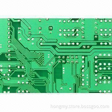
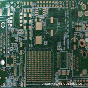
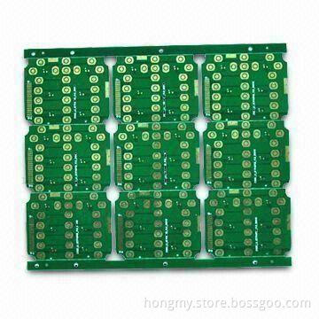
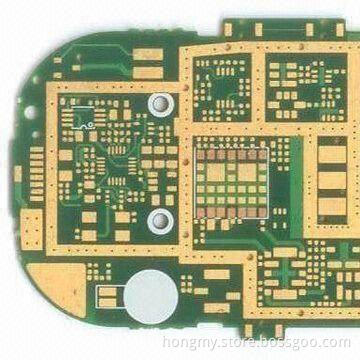
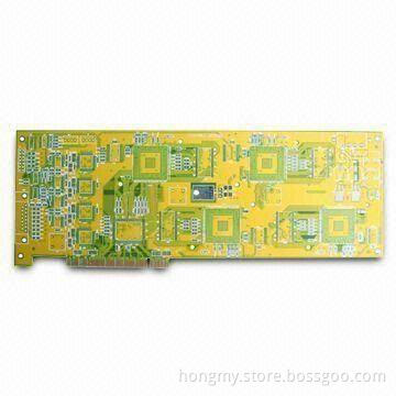
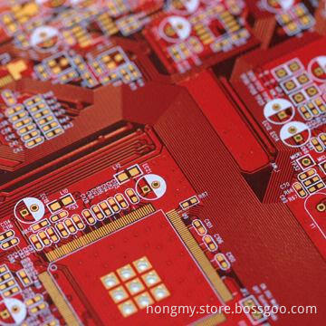
- Images:
- Minimum trace width (a): 0.075mm (3mil)
- Minimum space width (b): 0.1mm (4mil)
- Minimum annular ring: 0.1mm (4mil)
- SMD pitch (a): 0.2mm (8mil)
- BGA pitch (b): 0.2mm (8mil), 0.05mm
- Solder mask:
- Minimum solder mask dam (a): 0.0635mm (2.5mil)
- Solder mask clearance (b): 0.1mm (4mil)
- Minimum SMT Pad spacing (c): 0.1mm (4mil)
- Outer layer: 2oz
- Inner layer: 1oz
- Minimum trace width (a): 0.075mm (3mil)
- Minimum space width (b): 0.1mm (4mil)
- Minimum annular ring: 0.1mm (4mil)
- SMD pitch (a): 0.2mm (8mil)
- BGA pitch (b): 0.2mm (8mil), 0.05mm
- Minimum solder mask dam (a): 0.0635mm (2.5mil)
- Solder mask clearance (b): 0.1mm (4mil)
- Minimum SMT Pad spacing (c): 0.1mm (4mil)
Related Keywords
-

Double-sided PCB with 4oz Heavy Copper Thickness and Green Solder Mask

Four-layered PCB with 3oz Copper Thickness on all Layers and BGA Included

Double-sided PCB with 2.0 to 3.2 Board Thicknesses and Voltage of 10 to 300V

Multilayer PCB with Immersion Gold Surface and Green Solder Mask
Multilayer PCB with Immersion Gold and Heavy Copper, 1 to 20 Layers and 10 to 300V Test Voltage
Related Products-
FR-4 Gold Finger and LF-HASL Finish Multilayer PCB with 2oz Copper Thickness and 1.6mm Board
-
PCB Board, 610 x 508mm Panel Size, 1 to 16 Layers
-
Multilayer PCB with Immertion Gold Surface finish, FR-4 laminate
-
Double-sided PCB Circuit with FR4 Base and Immersion Gold Surface and 0.2mm Minimum Hole
-

Multilayer PCB with Green Solder Mask and 2 oz Copper Thickness
Product Categories-
Multilayer PCBs(310)
-
Double-sided PCBs(175)
-
High-density multilayer PCBs(144)
-
Aluminum PCBs(91)
-
Immersion gold PCBs(35)
-
Lead free HAL PCBs(27)
-
FR-4 PCBs(28)
-
Single-sided PCBs(28)
-
Copper PCBs(19)
-
PCB laminates(15)
-
OSP PCBs(10)
-
PCB assemblies(10)
-
Quick-turnaround PCBs(9)
-
Rigid-flex PCBs(3)
-
Double-sided flexible PCBs(2)
-
LED modules(1)


