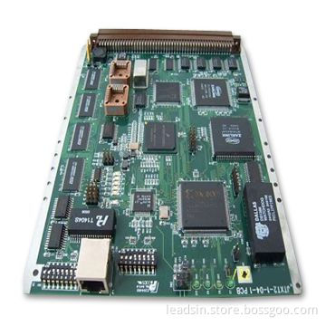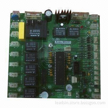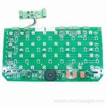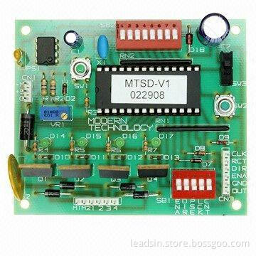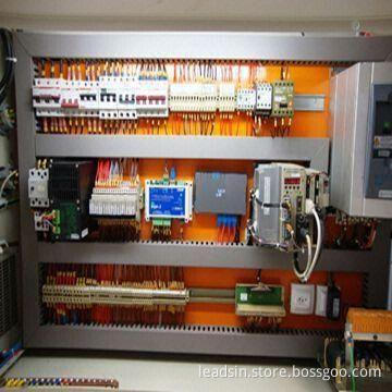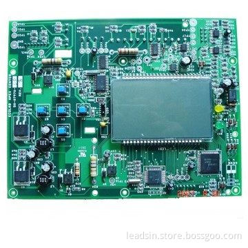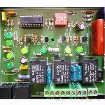
PCBA Design for Service/PCB Fabrication/PCB Assembly Service, Made of FR-4, Gold Finger Plating
- Payment Type:
- T/T, PayPal or L/C
Quantity:
Your message must be between 20 to 2000 characters
Contact NowBasic Info
Basic Info
| Payment Type: | T/T, PayPal or L/C |
|---|
Product Description
Product Description
- Layer: 1 to 22 layers
- Product types: rigid PCB, high-density inverter PCB, thick copper PCB
- Materials: FR-4, CEM-3, Teflon, aluminum substrate, Rogers, halogen free, high-Tg
- Copper thickness: 140 micron (4oz)
- Minimum board thickness: 0.4mm
- Maximum board thickness: 5.0mm
- Minimum finished hole diameter: 0.1mm
- Outer layer line width/spacing: 0.1/0.1mm
- Inner layer line width/spacing: 0.1/0.1mm
- Minimum aperture: 0.2mm
- Minimum laser drilling: 0.1mm
- Minimum ring width: 0.11mm
- Minimum BGA-bit hole spacing: 0.4mm
- Resistance tolerance: ±10%
- Minimum insulation thickness: 3-mil
- Maximum laser blind hole thickness to diameter ratio: 0.8:1
- Maximum working board size: 520 x 622mm
- Drilling tolerance (PTH): ±0.075mm
- Drilling tolerance (NPTH): ±0.05mm
- Outline tolerance (CNC): ±0.13mm
- Surface coating: lead-free HAL, HAL, flash gold, immersion gold, immersion tin, immersion silver, OSP, gold finger plating, carbon ink printing, peelable blue mask
- Double-sided PCB: 200,000ft2/month
- Single-sided PCB: 320,000ftsup>2/month
- HDI PCB: 80,000ftsup>2/month
- Comes with UL, SGS, RoHS marks
- Used to a wide range of fields such as computers, digital products, medical equipments, automobiles, communication devices, military, industrial controls and aviation
Related Keywords
Related Keywords
You May Also Like
You May Also Like

