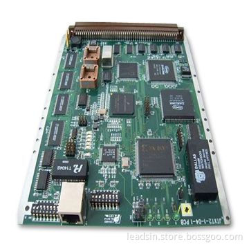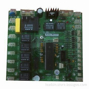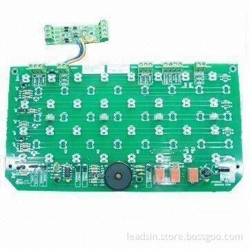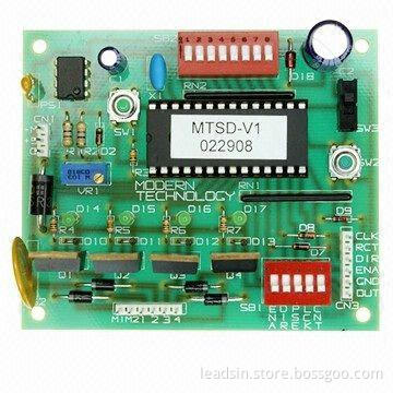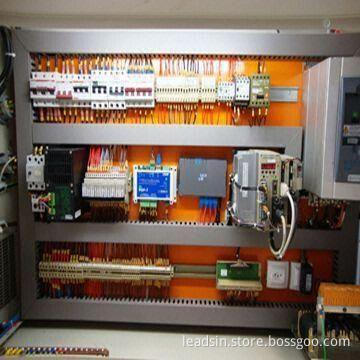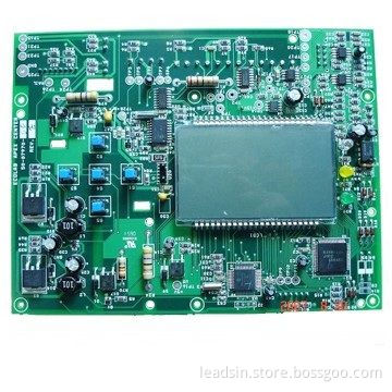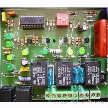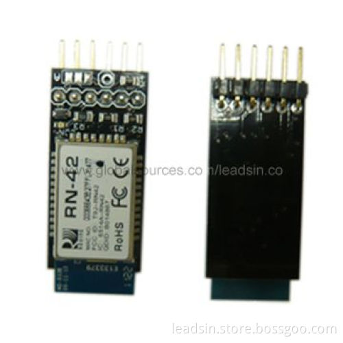
PCB Assemblies with Minimum Line Spacing/Width/Hole and 1 to 22 Layers
- Payment Type:
- T/T, PayPal or L/C
Quantity:
Your message must be between 20 to 2000 characters
Contact NowBasic Info
Basic Info
| Payment Type: | T/T, PayPal or L/C |
|---|
Product Description
Product Description
- Layers: 1 to 22
- Product type: rigid PCB, high density inverter PCB, thickcopper PCB
- Materials: FR-4, CEM-3, Teflon, aluminum substrate, Rogers,halogen free and high Tg
- Copper thickness: 140 micron (4oz)
- Board thickness: 0.4mm (minimum)
- Board thickness: 5.0mm (maximum)
- Finished hole diameter: 0.1mm (minimum)
- Outer layer line width/spacing: 0.1/0.1mm
- Inner layer line width/spacing: 0.1/0.1mm
- Aperture: 0.2mm (minimum)
- Laser drilling: 0.1mm (minimum)
- Ring width: 0.11mm (minimum)
- BGA-bit hole spacing: 0.4mm (minimum)
- Resistance tolerance: ±10%
- Insulation thickness: 3 mils (minimum)
- Laser blind hole thickness to diameter ratio: 0.8:1(maximum)
- Working board size: 520 x 622mm (maximum)
- Drilling tolerance (PTH): ±0.075mm
- Drilling tolerance (NPTH): ±0.05mm
- Outline tolerance (CNC): ±0.13mm
Related Keywords
Related Keywords
You May Also Like
You May Also Like

