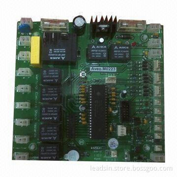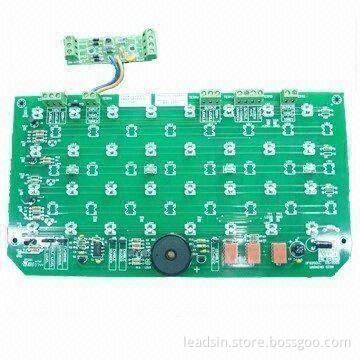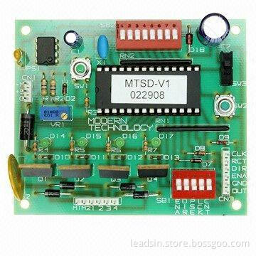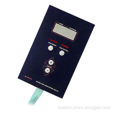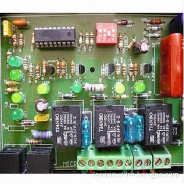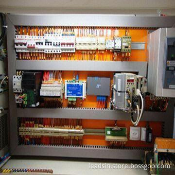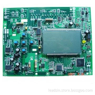
PBA clone service with full test
- Payment Type:
- T/T in Advance, L/C or PayPal
Quantity:
Your message must be between 20 to 2000 characters
Contact NowBasic Info
Basic Info
| Payment Type: | T/T in Advance, L/C or PayPal |
|---|
Product Description
Product Description
- We perform multiple quality assurance procedures before shipping out any PCB board
- These include:
- Visual Inspection
- Flying probe
- Bed of nails
- Impedance control
- Solder-ability detection
- Digital metallograghic microscope
- AOI (Automated Optical Inspection)
- Technical requirement for PCB assembly:
- Professional surface-mounting and Through-hole soldering Technology
- Various sizes like 1206, 0805, 0603 components SMT technology
- ICT (In Circuit Test), FCT (Functional Circuit Test) technology
- PCB assembly with UL, CE, FCC, RoHS approval
- Nitrogen gas reflow soldering technology for SMT
- High standard SMT and solder assembly line
- High density interconnected board placement technology capacity
- Quote requirement for PCB assembly:
- Gerber file and Bom list
- Clear pics of PCBA or PCBA sample for us
- Test method for PCBA
- Inner packing: vacuum package
- Outer packing: standard carton
- Finished boards are vacuum packed with bubble wraps and silica gel to prevent oxidization and damage during transportation, all the PCB will be checked before shipping
- PCB board: 5 to 7 days
- PCBA: 20 to 25 days
- Email us your PCB gerber files and Bom then we can quote for you
- Visual Inspection
- Flying probe
- Bed of nails
- Impedance control
- Solder-ability detection
- Digital metallograghic microscope
- AOI (Automated Optical Inspection)
- Professional surface-mounting and Through-hole soldering Technology
- Various sizes like 1206, 0805, 0603 components SMT technology
- ICT (In Circuit Test), FCT (Functional Circuit Test) technology
- PCB assembly with UL, CE, FCC, RoHS approval
- Nitrogen gas reflow soldering technology for SMT
- High standard SMT and solder assembly line
- High density interconnected board placement technology capacity
- Gerber file and Bom list
- Clear pics of PCBA or PCBA sample for us
- Test method for PCBA
Related Keywords
Related Keywords
You May Also Like
You May Also Like

