Shenzhen Leadsin Technology Co. Ltd
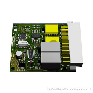
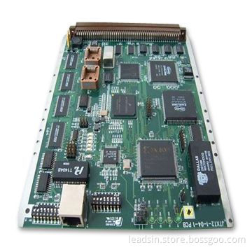
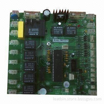
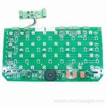
High-frequency PCBs with 1 to 30 Layers and 0.21 to 7.0mm Board Finish Thickness
  • High-frequency PCBs with 1 to 30 Layers and 0.21 to 7.0mm Board Finish Thickness
High-frequency PCBs with 1 to 30 Layers and 0.21 to 7.0mm Board Finish Thickness

High-frequency PCBs with 1 to 30 Layers and 0.21 to 7.0mm Board Finish Thickness

Payment Type:
T/T or L/C
Quantity:

Your message must be between 20 to 2000 characters

Contact Now
Basic Info
Basic Info
Payment Type: T/T or L/C
Product Description
Product Description
  • Agree PCB Gerber file
  • Fast prototypes delivery
  • One-stop for PCB design, copy, assembly, test, components
  • Lead-time: 7 to 10 days
  • PCB process capability
  • Layers: 1 to 30
  • Board finished thickness: 0.21 to 7.0mm
  • Materials: FR-4, CEM-1, CEM-3, high TG, FR4 halogen-free, rogers
  • Maximum finished board size: 23 x 25 (580 x 900mm)
  • Minimum drilled hole size: 3 mils (0.075mm)
  • Minimum line width: 3 mils (0.075mm)
  • Minimum line spacing: 3 mils (0.075mm)
  • Surface finish/treatment: HASL/HASL lead-free, HAL, chemical tin, chemical gold, immersion silver/gold, OSP, gold plating
  • Copper thickness: 0.5 to 7.0oz
  • Solder mask colors: green/yellow/black/white/red/blue
  • Copper thickness in hole: >25.0um (>1-mil)
  • Inner packing: vacuum packing/plastic bag
  • Outer packing: standard carton packing
  • Shape tolerance: ±0.13
  • Hole tolerance:
    • PTH: ±0.076
    • NPTH: ±0.05
    • Send your message to this supplier

      • Enter between 20 to 4,000 characters.

      Related Keywords

      Related Keywords
      Product Categories