
PCB
- Payment Type:
- T/T, Paypal, Western Union
Quantity:
Your message must be between 20 to 2000 characters
Contact NowBasic Info
Basic Info
| Place of Origin: | Jiangxi, China |
|---|---|
| Payment Type: | T/T, Paypal, Western Union |
Product Description
Product Description
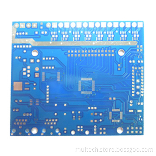
PCB Layer Number: 2
Board thicknesses: 1.0-1.6mm, 1.6- mm
Copper clad: 10Z/20Z/30Z
Surface technique: Lead-free HASL; OSP; Gold plated PBF HAL
Minimum hole size: 0.30mm
Minimum Line/Space: 0.2mm/0.2mm (4mil/4mil)
Solder mask: White/Black/Green/Red/Yellow/Blue/Gray...
Forming: Punching/CNC Milling/CNC V-CUT
PCB Testing: E-testing; Flying probe testing
Lead Time: Sample 5-7days; Mass production 7-15days
Payment: T/T(30% before production deposit 70% balance before deliver the order)


Related Keywords
Related Keywords


