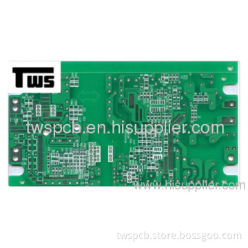
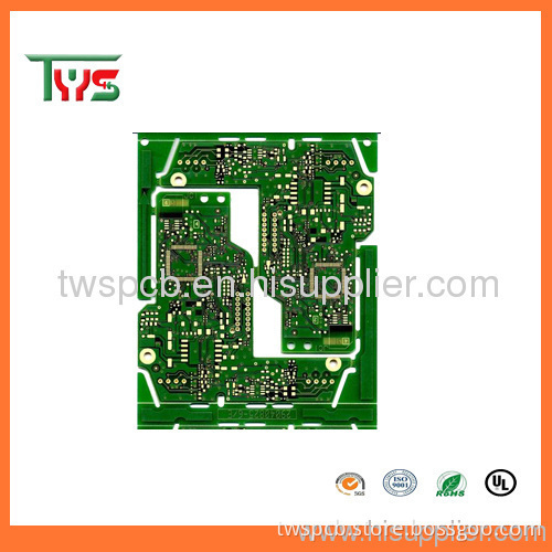


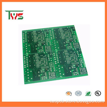
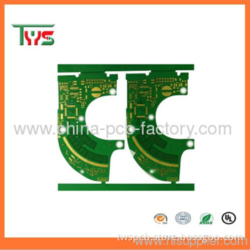
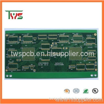
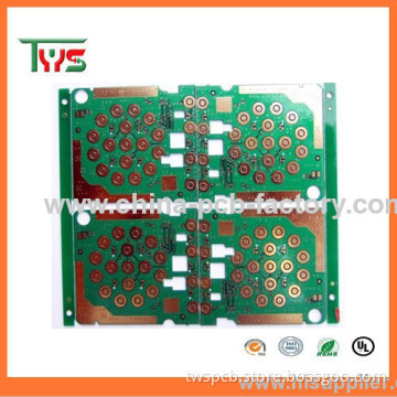
Multilayer Gold Immersion Oem Printed Circuit Board Pcb
Quantity:
Your message must be between 20 to 2000 characters
Contact NowBasic Info
Basic Info
Product Description
Product Description
Multilayer Gold Immersion OEM Printed Circuit Board PCB
------Tianweisheng Electronic Co.,Ltd
Why do youchoose us?
Why do youchoose us?
1. We have 20 years experienceprofessional PCB manufacturer.
2. Welcome your design, your logo can beprinted in the PCB.
3. We offer MOQ and samplingservice.
4. Our capacity can be 1000 squaremeter/square meters per month.
5. Sold makes types are according to yourrequirement (any color are available).
OurPCB Vision
Be the most reliable PCB and PCBA servicesupplier.
OurPCB Mission
1.Dedicate to satisfy customers'needs.
2.Provide high qualityproducts
3.Provide most professionalservices.
4.Deliver products ontime.
5.Keep all costs to minimum and maximizeour customers' benefits.
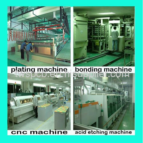
The PCB capability
We focus on high quality including quickturn PCB prototype , small volume, mid &Big volume PCB.
Capability:
-High Frequency (TACONICmaterial)/TG/Density/precision impedance controlled boards
-Heavy Copper PCB, Metal basedPCB. Hard Gold PCB, Blind &Buried vias boards,
Halogen Free PCB, Aluminum-backedBoards
-Gold finger+ HAL & Leadfree HASL PCB, Leadfree compatible PCB
PurchaseTips:
A.For PCB order,please provide Gerber file or *.pcb file. Any details are also welcomed if noGerber file.
B.Large PCB quantityorder, quotation will be based on SQM.
C.For PCBA order,please provide the Gerber file, *.pcb file and BOM List.
D.Reverse engineeringand PCB clone service can be supplied with your printed circuit boardsupplied.
E.Any questions,welcome to contact our sales person Ann by sending inquiry. Your satisfactionis our pleasure.

1> PCB ProcessingDetails:
Place ofOrigin shenzhen China(mainland) |
Brandname:TWS-PCB |
ModelNumber:4layer |
Basematerial:FR-4 |
Copperthickness:1oz |
Boardthickness:1.6mm |
Min.Holesize:0.2mm |
Min.linewidth:4mil |
Min. LineSpace:4mil |
SurfaceFinishing:immersion gold |
Soldermask:green |
Legend :White |
Test:E-testing |
.
2>PCB Package &Delivery:
Packdetails: |
Vacuumpacking,export carton |
Deliverytime: |
5-7days |
Productivity | ||
Item |
Technicalstandards |
|
Rise |
1-26layer |
|
Material |
CEM-1,CEM-3,FR-4,FR4TG170,TG180 ,HALOGEN FREE |
|
Lamellar |
0.2mm-3.20m(8mil-126mil) |
|
Minimumthickness |
0.1mm(4mil) |
|
Thick copper |
0.5-6 OZ |
|
Min line w / s |
0.075mm(3mil) |
|
Min Hole Side |
0.20mm(8mil) |
|
Min apertureChong |
0.9mm(35mil) |
|
Tolerance |
Hole drillingbit |
±0.075mm(3mil) |
Linewidth |
±0.05mm(2mil)Orwidth of ±20% |
|
Aperture |
PTH±0.075mm(3mil) |
|
NPTH±0.05mm(2mil) | ||
Shapetolerance |
MillingMachine±0.15mm(6mil) |
|
Punch±0.10mm(4mil) | ||
Warp |
0.70%-1.5% |
|
Pad surfacetreatment |
Nickel/Gold Finger Plating/FlashGold/Entek/LEAD Free Hal |
|
InsulationResistance |
10k-20MΩ |
|
Conductionresistance |
<50Ω |
|
Test voltage |
300v |
|
V Engraved |
Panle size |
110*100mm(min.)660*600mm(max.) |
Thickness |
0.6mm(24mil)min. |
|
Retention ofthe thickness |
0.3mm(12mil)min. |
|
Tolerance |
±0.1mm(4mil) |
|
Width |
0.50mm(20mil)max. |
|
Trough to aline |
0.5mm(20mil)min |
|
Trough |
Slot sizetlo.≥2WTolerance |
PTHL:±0.15mm(6mil) |
W:±0.1mm(4mil) | ||
NPTH:±0.125mm(5mil) | ||
W:±0.1mm(4mil) | ||
To circularfrom the hole |
PTH Hole:0.13mm(5mil) |
NPTH Hole:0.18(7mil) |
MLB |
Circulardeviation |
0.075mm(3mil) |
Deviationbetween layers |
4 layers:0.15mm(6mil)max |
|
6 layers:0.025mm(10mil)max. | ||
Aperture tothe smallest distance from theinner circle |
0.25mm(10mil) |
|
To circularfromthe hole |
0.25mm(10mil) |
|
ThicknessTolerance |
6 layers:±0.15mm(6mil) |
|
6 layers:±0.15mm(6mil) | ||
CharacteristicImpedance |
60Ω±10% |
|
If you send us your Gerber Filesand PCB specifications, we will quote for you within 12hours.
We always try our best! So we do,we conquer, and we get there!
Try us! You will findthat we are the right PCB supplier you want!


Related Keywords
Related Keywords