


Basic Info
Basic Info
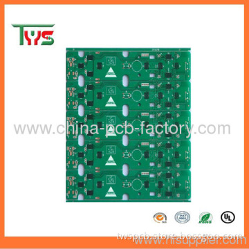
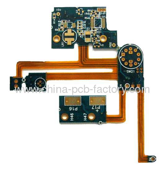
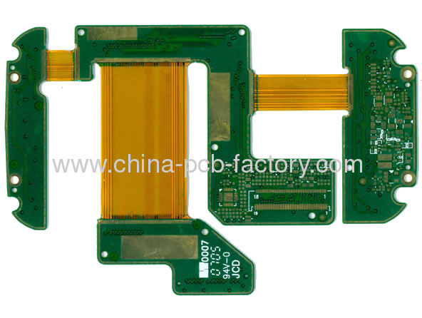
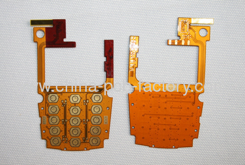
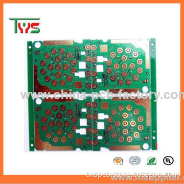
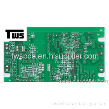
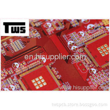
Product Description
Product Description
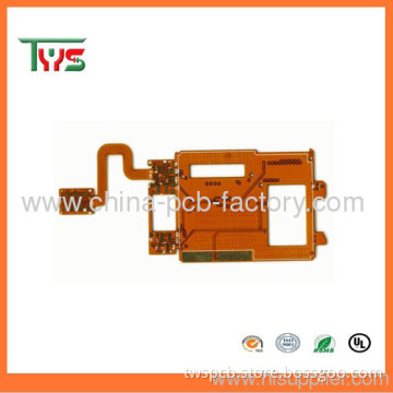
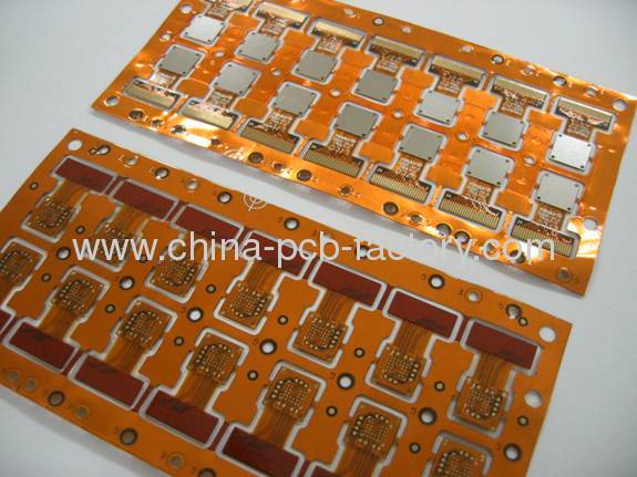
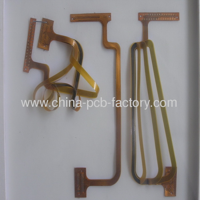
FPC with PI stiffener


Specifications:
1) Min. Trace width: 0.05 mm
2) Min. Space between trace: 0.07 mm
3) Min. Hole size: 0.1mm
4) Thickness tolerance:
A) Single sided: 0.005"
B) Double sided: 0.010"
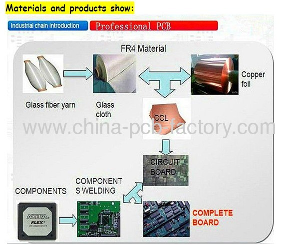
5) Base materials: Polyimide and polyester
6) Conductor (copper thickness): 13um~105um. (RA and ED copper)
7) Cover-layer: Polyimide and polyester (solder mask printing is available)
8) Adhesive material: Epoxy, acrylic and polyester
9) Stiffener materials: FR-4, mylar and polyimide
10) Surface finishes: ENIG,Plated gold ,OSP
1) Min. Trace width: 0.05 mm
2) Min. Space between trace: 0.07 mm
3) Min. Hole size: 0.1mm
4) Thickness tolerance:
A) Single sided: 0.005"
B) Double sided: 0.010"
5) Base materials: Polyimide and polyester
6) Conductor (copper thickness): 13um~105um. (RA and ED copper)
7) Cover-layer: Polyimide and polyester (solder mask printing is available)
8) Adhesive material: Epoxy, acrylic and polyester
9) Stiffener materials: FR-4, mylar and polyimide
10) Surface finishes: ENIG,Plated gold ,OSP
|
Production capacity production
|
Notes
|
|||
|
General ability
|
R & D
|
|||
|
Acceptance criteria
|
Product identification and performance specifications
|
The total PCB specificationIPC-6013 ClassⅡ,IPC-A-600G
|
/
|
Can consult the customer for the standard
|
|
Test Method
|
IPC-TM-650,GB/T4677-2002
|
/
|
|
|
|
Design software
|
Design software
|
CAM350,PROTEL,PADS2000,Powerpcb,GENESIS,ORCAD(Components required to provide a positive line of the drawing surface in order to check)
|
/
|
|
|
Gerber File Format
|
RS-274-D,RS-274-X
|
/
|
|
|
|
Drill file format
|
EXCELLONFormat(Figure holes)
|
/
|
|
|
|
Design
|
Layers
|
0-8Layer
|
9-12Layer
|
|
|
Thickness
|
0.07-4.0mm
|
/
|
|
|
|
Finished size of the largest
|
10X18 Inch
|
18X24 Inch
|
|
|
|
Smallest precision
|
±0.15mm
|
0.05mm
|
|
|
|
Laser
|
0.05mm
|
/
|
|
|
|
Steel
|
±0.1mm
|
/
|
|
|
|
Die cutter
|
±0.25mm
|
/
|
|
|
|
Hand shape
|
±0.5mm
|
|
|
|
|
Minimum of the positive degree of interlayer
|
8mil
|
/
|
|
|
|
Reinforcement plate fitting offset
|
±0.2mm
|
|
|
|
|
Journal of gold or gold patch the minimum distance between power
|
5mil
|
|
|
|
|
Minimum, single thickness,
|
0.07mm
|
/
|
plus1pcs CVL
|
|
|
One panel minimum line width / distance(1/3OZ,1/2OZAfter the copper-based compensation)
|
2/2MIL
|
/
|
|
|
|
One panel minimum line width / distance(1OZAfter the copper-based compensation)
|
3/3mil
|
/
|
|
|
|
Two-panel minimum thickness
|
0.16mm
|
/
|
Plus2pcsCVL
|
|
|
Double panel Minimum line width / spacing (base copper1/3OZ,Complete copper thickness<30um)
|
3/3MIL
|
/
|
|
|
|
Two-panel minimum line width / distance(1/2OZBase copper, finished copper thickness<35um)
|
3/3.5mil
|
/
|
|
|
|
Two-panel minimum line width / distance(1OZAfter the copper-based compensation)
|
4/4.5mil
|
/
|
|
|


FPC with PI Stiffener
Related Keywords
Related Keywords
You May Also Like
You May Also Like